Yenka simulator to build an RS flip-flop

Click For Summary
SUMMARY

The forum discussion focuses on building an RS latch using the Yenka simulator, specifically utilizing 2 NAND gates, switches, LEDs, and 330Ω resistors. Participants emphasize the importance of correctly wiring the circuit and adhering to the specified component requirements, including the necessity of a suitable power supply voltage, typically 3.3V or 5V. The distinction between an RS latch and an RS flip-flop is clarified, highlighting that a flip-flop is edge-triggered while a latch is level-sensitive. Participants also suggest improvements to the circuit diagram for clarity and functionality.

PREREQUISITES
  • Understanding of RS latch and RS flip-flop concepts
  • Familiarity with Yenka simulation software
  • Basic knowledge of digital logic design
  • Experience with circuit diagram conventions and resistor values
NEXT STEPS
  • Research the differences between RS latches and RS flip-flops
  • Learn how to simulate digital circuits using Yenka
  • Explore the implications of power supply voltage on logic gate performance
  • Investigate common practices for drawing circuit diagrams in digital electronics
USEFUL FOR

Electronics students, hobbyists building digital circuits, and educators teaching digital logic design concepts.

NYAME EPHRAIM
Messages
10
Reaction score
1
< Mentor Note -- thread moved to HH from the technical forums, so no HH Template is shown >

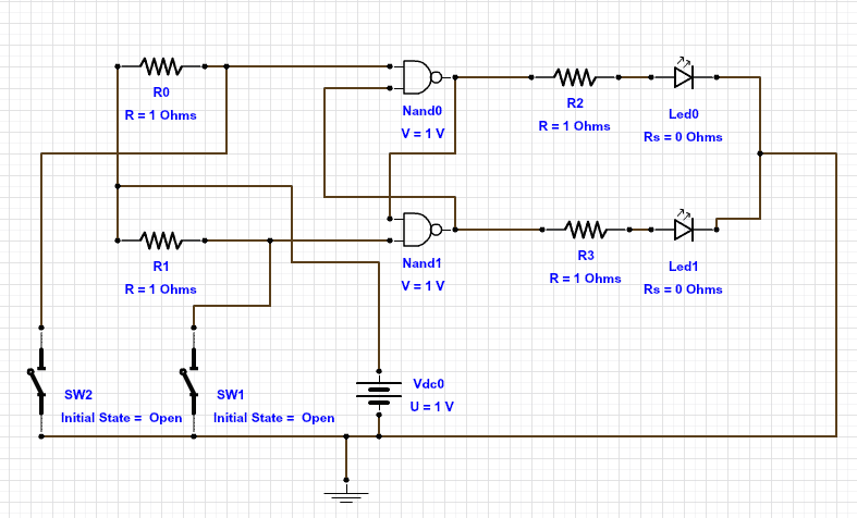
a) Using the Yenka (or similar) simulator, you are required to build an RS flip-flop using 2 NAND gates, switches, LEDs and 330Ω resistors. Test the circuit and prove its correct operation against the RS truth table, by print screening the 4 key modes and attaching a copy of your ‘RS flip-flop’ Yenka (or similar) file.

here is the diagram below i produced for the above task
Capture max follow up.PNG
 

Attachments

  • Capture max follow up.PNG
    Capture max follow up.PNG
    7 KB · Views: 770
Last edited by a moderator:
Physics news on Phys.org
So, where is your output? The only place I see where one would assume the output to be, you have tied back to ground.

Also, the left part of your circuit diagram is unnecessarily confusing and should be redrawn.
 
I moved this to a homework forum, which is more appropriate.

In the future, please use the homework forum and fill out the template. You did show us your work but you didn't ask a question.

p.s. Sorry @phinds, I cross posted with you.
 
NYAME EPHRAIM said:
330Ω resistors.
Your resistor values need updating. Also, are you using a 1V power supply rail on purpose?
 
berkeman said:
Your resistor values need updating. Also, are you using a 1V power supply rail on purpose?
Jeez, I was so struck by the lack of an output and the confusing way the circuit is drawn that I didn't even notice that. Glad to see someone here pays attention :smile:
 
  • Like
Likes   Reactions: berkeman
I should also point out that this is an RS-latch, not an RS-Flip Flop. A flip-flop is edge triggered (only changes state on a clock edge) but a latch can change output whenever the inputs change. This may seem like semantics but the different behaviors make a big difference depending on the kinds of circuits you want to build with this. Many arithmetic circuits, for instance, require flip flops to suppress glitches that can wreak havoc on the calculations.

In case you're interested, a common way to make a Flip Flop out of latches (common in school, not so common in practice) is to use two latches clock out of phase (you can generate the negative phase internal to your Flip Flop). That way, even though the two latches are asynchronous, the flip flop as a whole is edge-triggered.
 
  • Like
Likes   Reactions: berkeman
Hi @NYAME EPHRAIM, Welcome to PF.

Yes, your circuit very nearly meets the requirements stated in your first post. The overall wiring looks correct but a couple details need adjusting. The comments about the supply voltage do bring to mind that the supply voltage for the logic gates needs to be at least high enough to drive the output LEDs. I also noticed that you are not using the 330 Ohm resistors; is there a reason?

It seems some folks did not notice the "2 nand gate" requirement. I would truly like to see a flip-flop from the parts list you were given.

These days, most common logic circuits use either 3.3 or 5 Volts, and that is what they were expecting. However, over 15 years ago Texas Instruments came out with logic that works down to 0.8V. (http://www.ti.com/lit/ml/sceb011a/sceb011a.pdf)

Cheers,
Tom
 
I suspect the OP or his tutor meant latch when he wrote flip-flop.
 
This is a neater way to draw the switches...
DRDpI.png


The convention is to put higher voltage nodes (eg VCC or VDD) at the top and lower voltage nodes (gnd, 0V or -ve voltage rails) at the bottom of the drawing.
 

Attachments

  • DRDpI.png
    DRDpI.png
    5.5 KB · Views: 709
  • Like
Likes   Reactions: Tom.G and berkeman

Similar threads

  • · Replies 13 ·
Replies
13
Views
4K