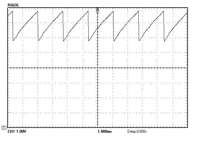
Quiz: Why/how does this circuit oscillate?

In summary, the circuit in Figure 1 measures the DC-coupled output waveform at 12V input. Only the frequency changes at different input voltages.
  • #1
gnurf
370
8
I hooked up a small circuit I found towards the bottom of this url and plotted the result in a spreadsheet (figure 1). Figure 2 shows the DC-coupled output waveform at 12V input. Only the frequency changes at different input voltages.

So what's going on here?

Figure 1:
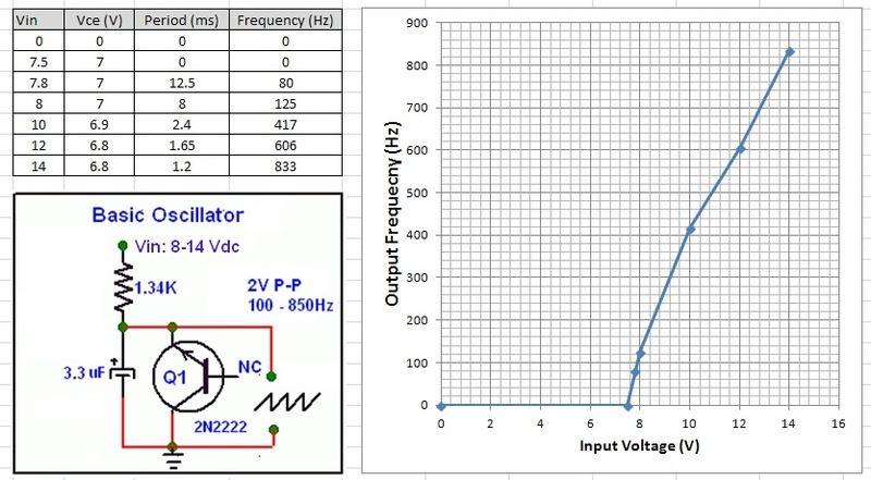
BrlIe.jpg


Figure 2:
2RwwL.jpg


Hint 1: Relaxation oscillator
Hint 2: http://www.eng.yale.edu/ee-labs/morse/compo/datasheets/2n2222.pdf
Hint 3: PN junction

EDIT - To avoid confusion: The Vce voltage from the table in Figure 1 is the 'DC' voltage measured with a multimeter.
 
Last edited:
Engineering news on Phys.org
  • #2
Research Unijunction transistor.

http://www.allaboutcircuits.com/vol_3/chpt_7/8.html
 
Last edited:
  • #3
nsaspook said:
I'm sorry, there's no price for copying the link from the top of the OP, but thanks for playing. :D

P.S I suspect you're over-qualified for this quiz.
 
  • #4
gnurf said:
I'm sorry, there's no price for copying the link from the top of the OP, but thanks for playing. :D

P.S I suspect you're over-qualified for this quiz.

Crap, I didn't even notice you had that same link in the OP. I just scanned the thread and remembered I'd seen the circuit before somewhere.
 
Last edited:
  • #5
It's the breakdown behaviour of bipolar transistors when the base is open. This voltage shows a hysteresis, because it take a minimum "base" current to have a current gain that reduces the breakdown voltage.

Many things are reverse polarized in your diagram. The capacitor can't be intentional. The transistor is probably intentional, in order to use the smaller base-emitter breakdown voltage. Though, as the reverse current gain is smaller, so is the hysteresis.

In real life, this would be more difficult to observe. I suspect the simulator introduces some "software" hysteresis by "deciding" if the junction avalanches.
 
  • #6
Enthalpy said:
It's the breakdown behaviour of bipolar transistors when the base is open. This voltage shows a hysteresis, because it take a minimum "base" current to have a current gain that reduces the breakdown voltage.

Many things are reverse polarized in your diagram. The capacitor can't be intentional. The transistor is probably intentional, in order to use the smaller base-emitter breakdown voltage. Though, as the reverse current gain is smaller, so is the hysteresis.

In real life, this would be more difficult to observe. I suspect the simulator introduces some "software" hysteresis by "deciding" if the junction avalanches.
Simulator? The circuit and waveform are real.
 
  • #8
There are so many oscillator circuits, I don't think I want to turn the NPN around and play with it like this. Do it the right way, tricks don't pay.

It is common knowledge that reversing the BE junction, you get a zener diode. But you don't do that because it's not meant to be and it's not guaranty that different parts behave the same, also degradation can happen if you use the part that's not designed to do, this is a no no in real world design. In real design, predictability and reliability is much more important than little wise tricks. Look up some simple oscillator circuits.
 
Last edited:
  • #9
Enthalpy said:
It's the breakdown behaviour of bipolar transistors when the base is open. This voltage shows a hysteresis, because it take a minimum "base" current to have a current gain that reduces the breakdown voltage.

It was a real circuit, not simulated, but apart from that Enthalpy's explanation is spot on. Well that is to say, it agrees entirely with my interpretation of the circuit. :smile:

A BJT will work with emitter-collector interchanged, but typically with very much reduced current gain and very much reduced breakdown voltage.
 
  • #10
But this hysteresis or should I say a negative resistance effect between collector and emitter junction. Occurs only for NPN transistor.

Long time ago I measure reverse-bias voltage from emitter to base and emitter to collector in general purpose BJT

attachment.php?attachmentid=53769&stc=1&d=1355048917.png


For PNP

BC556
Vbe=10V; Uce=10.65V

BD140

Ube=12.55V ; Uce=13.02V


And for NPN
BC337-40
Veb=8.2V; Vec=6.7V; I=5.5mA

BC549B

Veb=8.3V; Vec=7.2V; I=5.5mA

BD139-16

Veb=8.5V; Vec=6.7V; I=5.5mA

BC639

Vbe=7.7V; Vec=6.3V; I=500uA

BC337
Veb=7.9V; Vec=6,4V; I=500uA

2SC945
Veb=8.1V; Vec=7,5V; I=500uA

As you can see for NPN BJT's the Vec voltage is smaller than Veb breakdown voltage.

http://www.cappels.org/dproj/simplest_LED_flasher/Simplest_LED_Flasher_Circuit.html
 

Attachments

  • 2.PNG
    2.PNG
    2.5 KB · Views: 1,011
Last edited:
  • #11
Jony130 said:
But this hysteresis or should I say a negative resistance effect between collector and emitter junction. Occurs only for NPN transistor.

Thanks for sharing that info Jony. I suspect that the difference is not so much one of npn versus pnp, but rather due to differences in the reversed (c-e interchanged) current gain of the various transistors. I don't know if there's any systematic reason why pnp transistors would have a lower "reversed" current gain than npn types. Perhaps there is, though I can't think of anything off hand.

Current gain is usually relatively low in the "reversed" configuration, and if it is extremely low then we would expect little differences between the Vceo and Vcb breakdown voltages. This discrepancy (between the Vceo and Vcb breakdown voltages) is well known in both npn and pnp types, and in each case is due to the current amplification of the leakage in the Vceo (open cct base) configuration.
 
Last edited:
  • #12
gnurf said:
Simulator? The circuit and waveform are real.
My oops!

As Jony130 observed that
- the (small) reverse current gain does not drop the breakdown voltage of a PNP with open base,
- this is consistent with only NPN oscillating
- and with the explanation through (reversed) Vces and Vceo.

-----

The few times I tested a reverse beta for PNP, it has nothing shocking. There was some gain, not strikingly lower than for an NPN, so I suppose this is not a sufficient explanation.

-----

My complementary explanation, but it's not trivial.

Avalanche is not symmetric. To sustain itself, it needs new electrons and holes be brought in the impact zone, otherwise the avalanche is just blown away by lack of one carrier. This, in conjunction with a varying field strength, is used in some particle detectors (proportional avalanche) to multiply the charge without runaway.

Now, electrons are more efficient than holes to create new pairs. It's a matter of mass (similar to impedance matching, fit E and p instead of U and I) between already energetic carriers and the E and p of the bandgap.

Reverse-avalanche the emitter-base of an NPN: electrons are injected in the emitter, holes in the not-depleted base region, and at the limit holes don't create new electrons efficiently by impact. Now, these holes make a base current which the reverse beta can amplify, letting the collector inject fresh electrons in the base which supplement the inefficient impact of holes. So (reverse) beta helps an NPN avalanche.

In a PNP, electrons leave the depleted zone in the base, and these can create new holes by impact efficiently. So beta helps avalanche less in a PNP (a reversed PNP).

-----

There can be more reasons. Production processes aren't symmetric, for instance As (N dopant) diffuses very little in Si, B diffuses faster and P even faster, so As emitters achieve a steeper emitter profile that improves NPN transistors. Electrons are more mobile as well, and so on.

Current gain has much to do with doping profile and ratio (and very little with carrier lifetime, sorry books and teachers) so the reverse beta is not easy to justify. Compare doping in thee xpiaxial collector with doping in the base very near to the junction, and as well the dopant gradient within the base...
 

1. Why does this circuit oscillate?

The oscillation in this circuit is caused by the interaction of the components within the circuit. Specifically, the combination of a capacitor and an inductor creates a resonant circuit that allows for the continuous exchange of energy between them, resulting in the oscillating behavior.

2. How does the capacitor and inductor interact to create oscillation?

The capacitor and inductor work together to create a resonant circuit. The capacitor stores electrical energy in the form of an electric field, while the inductor stores energy in the form of a magnetic field. As the energy oscillates back and forth between these two components, it creates a continuous cycle of oscillation.

3. What is the role of the resistor in this circuit?

The resistor helps to control the flow of current in the circuit. It limits the amount of energy that can be exchanged between the capacitor and inductor, which helps to maintain the oscillation at a steady frequency.

4. Can the frequency of oscillation be adjusted in this circuit?

Yes, the frequency of oscillation can be adjusted by changing the values of the capacitor and inductor. A larger capacitor will result in a lower frequency, while a larger inductor will result in a higher frequency.

5. What are some real-world applications of circuits that oscillate?

Circuits that oscillate have a variety of practical applications, such as in radios, televisions, and electronic clocks. They are also used in electronic filters and sensors, and in communication systems for transmitting and receiving signals.

Similar threads

Replies
55
Views
3K
  • Introductory Physics Homework Help
Replies
3
Views
539
Replies
5
Views
2K
  • Electrical Engineering
Replies
6
Views
2K
Replies
12
Views
2K
  • Electrical Engineering
Replies
1
Views
971
  • Introductory Physics Homework Help
Replies
3
Views
237
  • Electrical Engineering
Replies
15
Views
3K
Replies
1
Views
959
  • Electrical Engineering
2
Replies
43
Views
5K
Back
Top