Analyzing the internal circuitry of IC 741 Op-Amp step by step

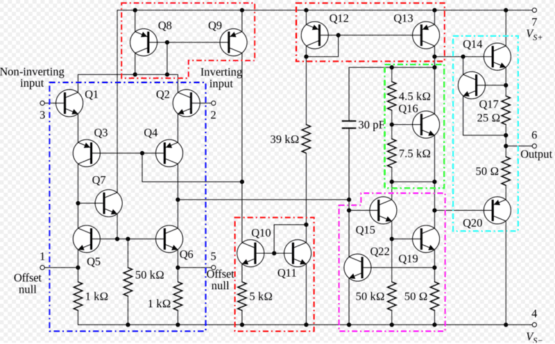
In summary, the dark blue block is a differential amplifier with emitter followers and common-base biased BJT's. The purple block is a voltage amplifier stage. The red block is a current mirror. The green block is a current amplification stage with low output impedance and a possible short-circuit protection. The cyan block is the output stage with low output impedance and high current gain. The input stage is provided by Q1 and Q2, which have emitter followers and current mirrors, respectively. The collectors of Q1 and Q2 are connected to the emitter and base of Q8, respectively. The differential amplifier's purpose is fulfilled by Q1,Q2,Q3 and Q4 only, and the entire dark
  • #1
PhysicsTruth
117
18
Homework Statement
(Not actually a homework) There are about 20 BJT's used in the internal circuit of a 741 op-amp, along with resistors and capacitors. I want to understand how this circuit works, and what role each BJT has to play. Sometimes, more than 1 BJT have to play a common role together.
Relevant Equations
Concepts to be used -
a) Differential Amplifiers
b) Wilson Current Mirror
c) Widlar Current Mirror
d) Emitter Follower
e) Darlington Pair
f) Voltage Amplifier (A or B class, probably)
Here is the internal circuit of a 741 op-amp -
use_3.png


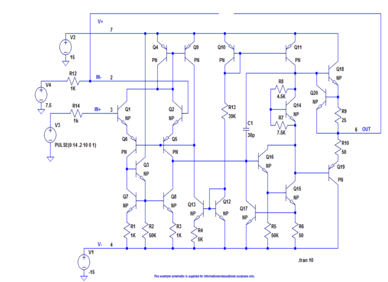
Here is a HSpice model I found in the educational section -
use_2.png


Both are essentially the same, keeping aside subtle differences. I am yet to understand the technicalities of an op-amp, so I would like to analyze the circuit using the first picture. The colored blocks represent the following, according to me-

a) Dark Blue - The input stage, a cascaded differential amplifier using emitter followers and common-base biased BJT's.
b) Purple - Voltage amplifier stage
c) Red - Current mirrors
d) Green - Current amplification with low output impedance, along with a possibly short-circuit protection.
e) Cyan - The output stage, with low output impedance, high current gain

The inputs are at Q1 and Q2, which serve as emitter followers. They are supposed to provide high input impedance for a high open loop voltage gain. Q8 and Q9 serve as the current mirror, where Q8 serves as the reference for Q9. Q3 and Q4 are matched with Q1 and Q2 respectively to ensure better ##V_{BE}## for protection, and also to increase frequency response. It seems that a feedback is sent to the bases of Q3 and Q4 from Q9's collector. Also, the collectors of Q1 and Q2 are connected to the emitter and base of Q8, respectively. What does this signify? I can't really seem to understand? I would like to take this step by step, so I would like someone to confirm at first if my hypothesis regarding the workings of Q1,Q2,Q3,Q4 are correct or not, or do they perform some additional roles as well? After that, I can move on with the next parts, otherwise if I make a mistake in the beginning, it would be difficult to analyze later on, especially with 20 BJT's around!
 
  • Informative
Likes Delta2
Physics news on Phys.org
  • #2
PhysicsTruth said:
Also, the collectors of Q1 and Q2 are connected to the emitter and base of Q8, respectively. What does this signify?
Respectively? I don't think so. Note that Q8 has B and C tied together, and supplies current to the Collectors of both Q1 and Q2.

If Q1, Q2 draw more current, Q9, being part of a current mirror, will pass more current cutting off Q3, Q4.

You thus have a negative feedback loop around the input stage, stabilizing the Q4 collector voltage; and maintaining an approptiate bias to Q15 - the output section.
PhysicsTruth said:
d) Green - Current amplification with low output impedance, along with a possibly short-circuit protection.
Q16, Green, is biasing to set the output stage (Q14, Q20) quiescent current, eliminating crossover distortion, probably class AB. (Enter the circuit in a simulator such as the free LTSpice to see all the bias points.)

The Output current limiting is done by Q17 and the 25Ω resistor. At roughly 28mA load current, Q17 turns On and diverts Q14s base drive. This eliminates any smoke signals when Q14 overheats from a shorted output.

Good Job!

Cheers,
Tom
 
  • Like
Likes PhysicsTruth
  • #3
Tom.G said:
Respectively? I don't think so. Note that Q8 has B and C tied together, and supplies current to the Collectors of both Q1 and Q2.

If Q1, Q2 draw more current, Q9, being part of a current mirror, will pass more current cutting off Q3, Q4.

You thus have a negative feedback loop around the input stage, stabilizing the Q4 collector voltage; and maintaining an approptiate bias to Q15 - the output section.

Q16, Green, is biasing to set the output stage (Q14, Q20) quiescent current, eliminating crossover distortion, probably class AB. (Enter the circuit in a simulator such as the free LTSpice to see all the bias points.)

The Output current limiting is done by Q17 and the 25Ω resistor. At roughly 28mA load current, Q17 turns On and diverts Q14s base drive. This eliminates any smoke signals when Q14 overheats from a shorted output.

Good Job!

Cheers,
Tom
Yeah, I had made a mistake in noticing Q8's common-base configuration.
Also, I would like to move on to the green block once I'm done with the previous blocks. Thanks for the explanations.
One thing I would like to ask - Is the differential amplifier's purpose fulfilled by Q1,Q2,Q3 and Q4 only, or does the entire dark blue block functions as a differential amplifier as a whole? Like, what exactly happens in the input stage if we put in differential inputs at the terminals of Q1,Q2 ?
 
  • #4
PhysicsTruth said:
Yeah, I had made a mistake in noticing Q8's common-base configuration.
Also, I would like to move on to the green block once I'm done with the previous blocks. Thanks for the explanations.
One thing I would like to ask - Is the differential amplifier's purpose fulfilled by Q1,Q2,Q3 and Q4 only, or does the entire dark blue block functions as a differential amplifier as a whole? Like, what exactly happens in the input stage if we put in differential inputs at the terminals of Q1,Q2 ?
Also, the next part in the dark blue block seems to be a Wilson current mirror with an active load driven by Q7. So, does Q3 act as a current source in this case, as there is no resistor, which is present in a typical Wilson current mirror? So, is the input circuit functioned to act as a current source?
 
  • #5
PhysicsTruth said:
Yeah, I had made a mistake in noticing Q8's common-base configuration.
Q8-Q9 are connected the same as Q12-Q13 and Q8 is the reference for the current source Q9. See:
https://wiki.analog.com/university/courses/electronics/text/chapter-11

PhysicsTruth said:
Also, the next part in the dark blue block seems to be a Wilson current mirror with an active load driven by Q7. So, does Q3 act as a current source in this case,
Q5,6,7 are a Buffered Current Mirror, see sect. 11.7 in the link above.
And yes, I would consider Q3 to be the current source for Q5,6,7.

You can probably figure out the answers to many of your questions, and learn a lot more, if you get a free copy of the LTSpice simulator from:
https://www.analog.com/en/design-center/design-tools-and-calculators/ltspice-simulator.html

It is pretty easy to use once you get started. You can enter your opamp schematic using the generic NPN and PNP transistors that are part of the download library. It's great for probing voltages and currents at various points by connecting a virtual meter to the point of interest. Many of us on this site use it for quick circuit design and evaluation.

And here is a download that seems to describe the separate operational stages of the 741. I've only glanced at it, so no guarantees!
https://cdn.evilmadscientist.com/KitInstrux/741/741_principles_RevA104.pdf

Cheers,
Tom
 
  • Like
Likes PhysicsTruth

1. What is an IC 741 Op-Amp?

The IC 741 Op-Amp is a type of integrated circuit that is commonly used in electronic circuits to amplify and process analog signals. It is a versatile and widely used component in various electronic devices, such as audio amplifiers, filters, and voltage regulators.

2. How does the internal circuitry of an IC 741 Op-Amp work?

The internal circuitry of an IC 741 Op-Amp consists of several transistors, resistors, and capacitors that work together to amplify and process analog signals. The input stage of the Op-Amp amplifies the input signal, while the output stage provides a high gain output signal. The feedback network helps to stabilize and control the gain of the Op-Amp.

3. What are the steps to analyze the internal circuitry of an IC 741 Op-Amp?

The following are the steps to analyze the internal circuitry of an IC 741 Op-Amp:

  1. Identify the components in the circuit, such as transistors, resistors, and capacitors.
  2. Determine the function of each component in the circuit.
  3. Draw a simplified circuit diagram of the Op-Amp, including the input and output stages, feedback network, and power supply connections.
  4. Analyze the circuit by applying basic circuit laws, such as Kirchhoff's laws and Ohm's law.
  5. Calculate the gain and other parameters of the Op-Amp based on the circuit analysis.

4. What are some common issues that can occur in the internal circuitry of an IC 741 Op-Amp?

Some common issues that can occur in the internal circuitry of an IC 741 Op-Amp include:

  • Offset voltage: This is an error voltage that can affect the accuracy of the output signal.
  • Input bias current: This is a small current that flows into the input terminals of the Op-Amp, which can cause errors in the output signal.
  • Input offset current: This is a difference in the input bias currents of the two input terminals, which can also affect the accuracy of the output signal.
  • Frequency response: The Op-Amp may have limited bandwidth, which can result in distortion or attenuation of high-frequency signals.

5. How can I troubleshoot issues with the internal circuitry of an IC 741 Op-Amp?

To troubleshoot issues with the internal circuitry of an IC 741 Op-Amp, you can:

  • Check the connections and ensure they are correct and secure.
  • Test the components in the circuit to make sure they are functioning properly.
  • Use a multimeter to measure the voltages and currents in the circuit and compare them to the expected values.
  • Check for any damaged or faulty components and replace them if necessary.
  • Refer to the datasheet for the Op-Amp and make sure it is being used within its recommended parameters.

Similar threads

  • Engineering and Comp Sci Homework Help
Replies
2
Views
2K
  • Engineering and Comp Sci Homework Help
Replies
4
Views
2K
  • Engineering and Comp Sci Homework Help
Replies
1
Views
2K
  • Engineering and Comp Sci Homework Help
Replies
3
Views
2K
  • Engineering and Comp Sci Homework Help
Replies
32
Views
3K
  • Engineering and Comp Sci Homework Help
Replies
13
Views
2K
  • Engineering and Comp Sci Homework Help
Replies
24
Views
2K
  • Engineering and Comp Sci Homework Help
Replies
5
Views
1K
  • Engineering and Comp Sci Homework Help
Replies
13
Views
2K
  • Engineering and Comp Sci Homework Help
Replies
8
Views
3K
Back
Top