Common mode current simulation

In summary, the two models are not comparing well because the generator in the first model has more series resistance. You need a 2 msec transient analysis time, not 2 microsec; .tran 2m.
  • #1
Mathhhew
20
1
TL;DR Summary
Two software give differents results with the same circuit
Hello!

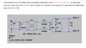
I'm trying to model common mode current with LTSpice, but there is a problem with my simulation. Someone else tried on an other software and got the expected result, but I can't explain why. When going through the capacitor, square signals should become pulses, but that's not the case for me Here is the two screenshots:

This is the one that shows the expected results
image4814.PNG


and mine
comparaison.png
 
Engineering news on Phys.org
  • #2
You have missed part of the LTspice schematic circuit in the post. There are no inductors ?
LTspice has assumed parameters for inductors that are not shown on the screen.
You need to post the CM_generator.asc file, but as a text file; CM_generator.asc.txt
Then I can look at what is not shown.
 
  • Like
Likes berkeman
  • #3
You are simulating the circuit 2000 times faster than the other model. 1 usec ~ 2 millisec cycle.
V1 should be PULSE(0 10 0 10u 10u 0m5 1m0)
Why is V1 "Rser=50" when in series with 100R ? make it Rser=0

You need a 2 msec transient analysis time, not 2 microsec; .tran 2m
 
  • Informative
  • Like
Likes DaveE and berkeman
  • #4
Hello!
Baluncore said:
V1 should be PULSE(0 10 0 10u 10u 0m5 1m0)
I assume that was the problem, because now it matches the other graph, thanks!

Baluncore said:
Why is V1 "Rser=50" when in series with 100R ? make it Rser=0
I need the internal resistance, otherwhise current at R3 is constant without any perturbation

Capture d’écran 2022-01-08 222348.png

(now it works :)
 
  • #5
Mathhhew said:
I need the internal resistance, otherwhise current at R3 is constant without any perturbation
You have reversed the numbering of the voltage sources between the competing diagrams. I refer to the pulse generator on the left. Yours has 50R internal + 100R external = 150R extra in series with the pulse generator, before the split in two, each branch of which has 100R.

The models should not have the same response since your generator has more series resistance.

Screen dumps make it very difficult to diagnose what is what.
Only an LTspice.asc as an attached .txt file can be trusted.
 
  • #6
Hello
yes you're right I confused the two generators. The resistance was only here to measure the intensity created by the generator, because back then, I had a problem, I couldn't measure it directly from V1. Anyway I just deleted it. here's also the txt file you requested
 

Attachments

  • CM_generator.asc.txt
    1.4 KB · Views: 114
  • #7
I made some minor changes.
Faster edges for V1. Remove V1 Rseries=50R, by making it zero.
Then I(V1) better matches the other model.
Remove units F and s from values. Value F is femto, not farad. s is redundant.
 

Attachments

  • CM_gen_edit 1.asc.txt
    1.4 KB · Views: 116
  • CM_gen_edit 1.plt.txt
    296 bytes · Views: 116
  • #8
Hello

So I ran into a problem when I tried to plug the CM filter. What I did is to model the choke with a 1:1 transformer and then add two capacitor to complete the filter. But that doesn't work as expected. Instead of a continuous intensity, I'm getting some weird oscillations, and I don't know how to fix that.

lpb.png
 

Attachments

  • CM_gen_edit_with_choke.asc.txt
    2 KB · Views: 122
  • #9
Your input square wave is “plucking” the LC circuit and causing it to ring.
Your output voltage had one side grounded to satisfy DC bias, but input was asymmetric. Now it uses two 1G resistors.
Plot the 'in' voltage and the output differential voltage.
 

Attachments

  • CM_gen_edit_with_choke_1.asc.txt
    2.4 KB · Views: 126
  • CM_gen_edit_with_choke_1.plt.txt
    340 bytes · Views: 128
  • #10
ok so there was a conflict with the ground. Still I have two question: what are the two resistors for? Because I've tried without and I saw no difference. And I don't understand the word "plucking"😅
 
  • #11
Mathhhew said:
Still I have two question: what are the two resistors for?
Each node in a spice circuit must have a DC voltage reference path to ground. When I removed the ground from the output I referenced the right hand side of the circuit to ground through two 1G resistors. Capacitors block DC currents, so are treated as open circuit during the initial DC operating point analysis. It is a weird behaviour, but LTspice may sometimes be happy with the DC analysis if the resistor was there earlier, but when you save and run again, it finds the DC bias problem.

Mathhhew said:
And I don't understand the word "plucking"
Plucked, like a harp or a banjo. The sharp edges of your square wave have wide band frequency harmonic contents. I think it was the input caps C1 and C2 that were resonant with the L1:L2 CM choke inductance, (seen through the 100 ohm resistors and against the output ground). Remove C3 and C4, or make them one pF, to see how much of a part they played in the resonance. Change R1 and R2 to see if they change the attenuation of the ringing following each step edge of the input.

I am looking for a different CM choke testing circuit that will be better behaved and easier to understand. Once I have refined it, I will post it here.
 
  • #12
Here is a different simulation that allows common mode and differential signals to be tested.

The normal mode signal is a differential signal from Vs, with the image generated by E1. The common mode noise comes from Vcm and is applied to the mid-point of the differential signal.

Line resistance Rs, and choke inductance Lt, are parameters that keep the circuit balanced as you experiment with how far you can push them before the performance is degraded.

This circuit can be changed to simulate several different things.
Run a 2ms .tran analysis and view the signal input against output.
Run a 20ms .tran analysis, select plot window, then view, and FFT, to show cm rejection ratio.
Change Vcm to AC 1 and do an .ac analysis to see cm rejection across frequency.
Similarly, make Vs an AC 0.5 source to see .ac analysis of the signal path.
Note that the differential signal is doubled if not AC 0.5, so it has a +3 dB gain if AC 1 is used.
CMgen_4.png
 

Attachments

  • CMgen_4.asc.txt
    2.3 KB · Views: 120
  • CMgen_4.plt.txt
    332 bytes · Views: 112
  • #13
Thank you for your answer, it helps a lot!

What happened to the two capacitor I previously had in serie with R1 and R2? Were they useless?

And back on my previous circuit, the guy who gave me the circuit said that I would be able to see oscillations at the beginning of the filtered signal, showing the usefulness of a resistor to attenuate these oscillations, as seen in the picture. But I don't have these oscillations, my filtered signal is smooth right away, and I don't understand why.
Rdump.PNG

I don't have the time right now to do everything you said, but I'll try as soon as possible (and maybe come back with an other set of questions :p)
 
  • #14
Mathhhew said:
What happened to the two capacitor I previously had in serie with R1 and R2? Were they useless?
The series C made it too difficult to identify what was influencing the response. They also caused the unreal AC floating island that later needed to be ground referenced with the 1G+1G resistors. The complexity increased again when your signal source had a fixed hidden internal resistance that was not compatible with all signal and power applications of CM chokes.

As an example of making it simpler, in the latest circuit you post in #13, there is a low impedance voltage source, V2, driving R2+C2 against ground, and you are measuring the V2 current, which is confounded by the addition of that unnecessary frequency dependent current component.

I directly generate and sum two low impedance voltages, that are opposite phases of the signal, but have identical common mode noise. The series Rs in my circuit represents the impedance of the source and cables. The inductance of the CM choke can be selected, with additional components if needed. The output load, Rd, can be chosen to represent the appropriate signal input or low impedance power supply rails that are being driven by your CM choke model.

I have now changed my load to use a centre-tap grounded pair of load resistors. That makes for symmetry, so only one output resistor (Rd) needs to be considered, which corrects for the +3 dB double signal source. Set the parameters of the model with “.param Rs=1 Lt=2m Rd=100”. Now that the source impedance R+C has been eliminated, it is the ratio of only those three parameters that represent the real world circuit and determine the transfer function of the CM choke being modeled over the specified AC frequency range.

Mathhhew said:
But I don't have these oscillations, my filtered signal is smooth right away, and I don't understand why.
Probably because the 10 uF output caps swamp the 100 nF coupling caps, making the input more like a current source. The resonant frequency is decided by choke Lt and the two coupling caps, while oscillation is damped by the load resistance.

P.S. Note that a square wave with longer rise and fall times will have less high frequency energy and so will cause less ringing.
 
Last edited:
  • #15
Hello

Is there a way to use LtSpice to simulate "real" common mode current? I know that buck converter for example produce common mode mode current, and I thought comparing a real system to our "homemade" model might be quite relevant, but I began using Lt spice with this project, so I'm not really on point with all the things you can do with it. And where can I import a common mode choke in LtSpice? Because I've seen pictures with it, but I can't find it on my software
 
  • #16
Mathhhew said:
And where can I import a common mode choke in LtSpice? Because I've seen pictures with it, but I can't find it on my software
CM chokes are normally built from two coupled inductors, with parallel tracks drawn between them to represent the core.
Can you please give me a link to a picture of a dedicated CM choke component.
 
  • #17
Sure
From https://www.allaboutcircuits.com/technical-articles/designing-and-simulating-emc-filters-ltspice/
 

Attachments

  • 232856.png
    232856.png
    29.7 KB · Views: 116
  • #18
  • #19
Hello!

So I've ploted the bode diagram of a filter and I've obatined a weird result: some kind of resonance (we clearly see it on the phase plot, less on the gain plot)
resonance.png


But it only appears when I've added the ground to the generator, and I'm not sure if it is really needed (the new reference point)
ground.png


appart from that, I've also ploted the bode diagram without a common mode choke, but with two uncoupled inductors with the same value as the choke , and I can't explain the difference between the two of them. Of course I knew I would get two different plot, because the component aren't the same, but from a mathematical point of view, the transfer function is the same: two parallel inductors and two capacitors. I can't figure out the impact of the coupled inductors in the transfert function, and how to express mathematically the difference between both of them

Both.png


red is without the chokethanks in advance for your help
 

Attachments

  • CM_gen_edit_with_choke_1.asc.txt
    5.4 KB · Views: 123
  • #20
There is no CM signal component in your model.
If you are modelling a power supply filter, then you don't need a 50 ohm series resistor in the V3 supply.
Also you don't need a balanced differential signal output for a power supply.
 
  • #21
Here are a couple of AC analysis files, one for CM rejection, and one for signal transfer.
There are only three parameters to juggle initially.
There are no capacitors to ring with the choke, or to require fake grounds.
Notice that signal attenuation is about 0.1 dB due to the ratio of Rd /( Rd+Rs ).
Notice that signal phase is less than a milli degree.
The signal is doubled, but then only the top half is analysed, so dB is correct.
I believe that is as simple as analysis of a CM choke can get.
 

Attachments

  • CM_rej.plt.txt
    595 bytes · Views: 111
  • CM_rej.asc.txt
    2.5 KB · Views: 99
  • CM_sig.plt.txt
    621 bytes · Views: 108
  • CM_sig.asc.txt
    2.5 KB · Views: 112
  • #22
Baluncore said:
you don't need a 50 ohm series resistor in the V3 supply.
I did what you've said and indeed it looks better :)But I don't understand why the resistance was the problem. In a real montage, I would have this serie resistance, so shouldn't I include it to be closer to the real montage?

Mathhhew said:
I can't figure out the impact of the coupled inductors in the transfert function, and how to express mathematically the difference between both of them
And I'm still interested to know that, because I still have a difference between both of them
Both.png

red one is without the CM choke
 

Attachments

  • CM_gen_edit_with_choke_1.asc.txt
    4.8 KB · Views: 114
  • #23
Baluncore said:
There are no capacitors to ring with the choke, or to require fake grounds.
Right, but in a second order filter, capacitors are required

When you plot the bode diagram, why aren't you using only an AC generator (without the CM generator)?

And last, It is the first time that I see this kind of diagram (the rejection one), so I don't really understand what I should notice
 
  • #24
Mathhhew said:
Right, but in a second order filter, capacitors are required
They will be in parallel, not series.

Mathhhew said:
When you plot the bode diagram, why aren't you using only an AC generator (without the CM generator)?
The unimportant voltage source is a low impedance that completes the AC model of the circuit.

Mathhhew said:
And last, It is the first time that I see this kind of diagram (the rejection one), so I don't really understand what I should notice.
You are interested in the differential signal getting through, without contamination by the CM noise. To study that you excite a CM signal and look to see how much is transferred to the output.

Re: Your circuits attached to post #22.
Out is a LPF of the 50 ohm with capacitance. 90 deg phase. No a resonance.
Out2; I cannot immediately explain the resonace near 15 MHz.
Out3 as expected shows the resonance of 26 mH in series with 5 uF at 441.6 Hz.
A CM choke is effectively wound back on itself, which cancels the differential mode magnetic field and the circuit inductance. Without the coupling coefficient the CM choke is gone, but the choke inductance appears twice in the series circuit.

PS Edit.
The 15 MHz resonance of Out2 appears to be an artefact of the computation. The currents in L3 and L4 do not cancel completely because of the floating point precision used. That results in a small residual choke inductance that resonates with the output capacitance. The resonance can be moved by changing the parameters Lcm=13mH, or Cp=10uF, or K=0.999999
 
Last edited:
  • #25
I'm sorry but I still don't understand what am I looking at. There's too much spikes and the phase is going from -8K° to 10K° seems absurd (is it 10 kilo degree?)
rej.png
 
  • #26
That is not what I see. All your signal is below -300 dB. I think you are looking at two very small signals that add and subtract randomly to generate phase reversals. Do not use the subtraction V(out,_out)
Look at only V(out). Do NOT reference the plot to _out.
 
  • #27
You're right that's better
better.png
:smile:
thanks!
 
  • Like
Likes Baluncore

1. What is common mode current simulation?

Common mode current simulation is a type of simulation used in electrical engineering to analyze and predict the effects of common mode currents on a system. Common mode currents are currents that flow in the same direction through multiple conductors, and can cause interference and other issues in electronic systems.

2. Why is common mode current simulation important?

Common mode current simulation is important because it allows engineers to identify potential issues and make design changes before a system is built. This can save time and money, as well as prevent problems such as electromagnetic interference (EMI) and signal distortion.

3. How is common mode current simulation performed?

Common mode current simulation is typically performed using specialized software that models the behavior of common mode currents in a system. This software takes into account factors such as the layout of conductors, the properties of materials, and the frequencies of the currents.

4. What are some common applications of common mode current simulation?

Common mode current simulation is commonly used in the design of electronic systems, including printed circuit boards, power supplies, and communication systems. It is also used in the development of medical devices and industrial equipment.

5. What are some challenges in common mode current simulation?

One of the main challenges in common mode current simulation is accurately modeling the behavior of the system. This requires a thorough understanding of the physics and electrical properties involved. Additionally, the complexity of modern electronic systems can make it difficult to accurately simulate all potential scenarios.

Similar threads

Replies
7
Views
1K
Replies
1
Views
963
Replies
9
Views
4K
Replies
93
Views
5K
  • Electrical Engineering
Replies
15
Views
4K
  • Electrical Engineering
Replies
14
Views
812
  • Electrical Engineering
Replies
4
Views
2K
  • Electrical Engineering
Replies
10
Views
1K
Replies
14
Views
2K
Replies
21
Views
4K
Back
Top