Small signal AC modeling for a boost converter with resistive losses

In summary, the conversation discusses the issue of eliminating "I" in the final inductor and capacitor equations in a boost converter problem. The solution is explained in detail, using small-signal AC modeling and steady-state equations to express the quiescent inductor current in terms of other parameters, thus eliminating "I" in the equations. There is also a discussion about the use of Vg instead of V to express the voltage conversion ratio in the problem.
  • #1
pjcircle
15
0
Homework Statement
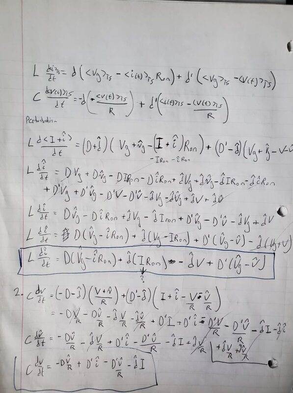
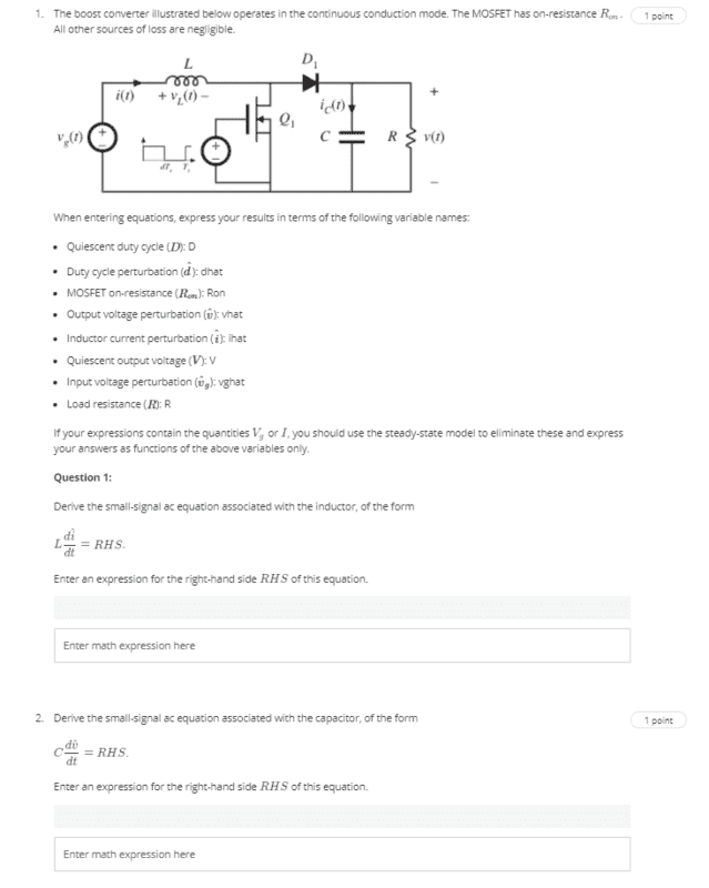
Derive the small signal equations associated with both the capacitor and inductor.
Relevant Equations
L dihat/dt=RHS
C dvhat/dt=RHS
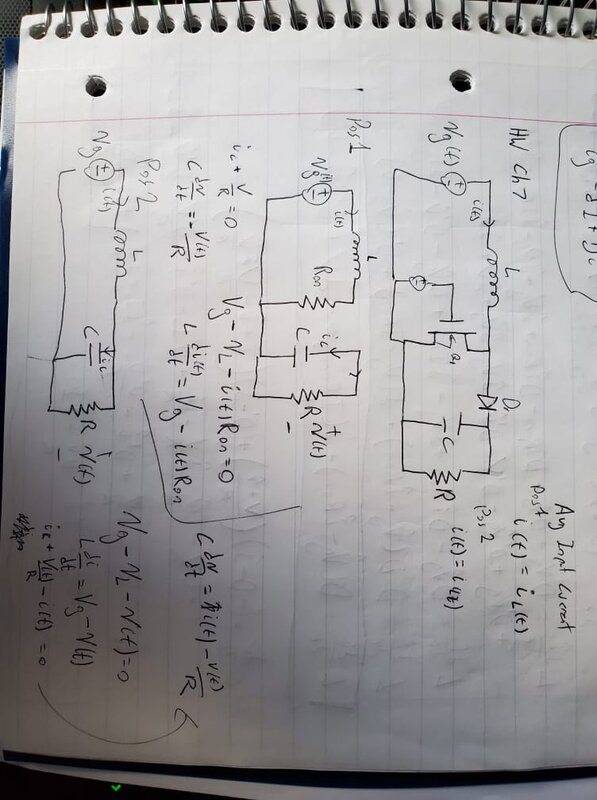
I've attached my attempts at the solution and the actual question below. I believe the only issue I am having is I don't know how to get rid of "I" in both my final inductor and capacitor equations as the HW states I shouldn't have anything in term of I. I believe I need to put "I" in terms of the listed variables but I cannot for the life of me figure out how to do it. In the lectures and textbook that come with this HW they do actually leave the solution with terms that include "I" which is a bit frustrating. I already removed the second order and DC quantities as can be seen in the work but "I*Ron*dhat" and "dhat*I" are first order factors that should not be removed. The blue boxed in equations in third image are my incorrect answers for #1 and #2.
unknown.png
hw1.jpg
hw2.jpg
 
Physics news on Phys.org
  • #2
I did not study your derivation process in detail. However, I think in a sense, you can’t get rid of "I". The small-signal AC model of the boost converter must actually include the influence of the quiescent inductor current, but, as mentioned in the HW, according to the steady-state model, you should be able to use other parameters to represent it. You may try to consider whether this quiescent inductor current is related to, for example, the output voltage and some other parameters?
 
  • #3
I don't think your equations are correct. First of all, since the convertor operates in continuous current mode, the average (over a switching period) inductor current equals average current throug the diode when it conducts.

Let us define I(t) - inductor current averaged over a switching period, ##V_g(t)## - source voltage, V(t) - output voltage (averaged over a switching period). These can be written as I(t) = I + i(t), ##V_g(t) = V_g + v_g(t)##, and V(t) = V + v(t) where I, ##V_g## and V are quiescent values and small letters denote perturbations.
Then the FET is on, the voltage across it is ##I(t) R_{ON}##. During off time and assuming negligible voltage drop across the rectifying diode, the voltage is equal to the output voltage, V(t). The average (over the switching period) voltage is then ##I(t)R_{ON}D(t) + V(t) \cdot (1-D(t))##
We can then write the equation for the diode current as
$$V_g (t) - I(t)R_{ON}D(t) - V(t)\cdot (1-D(t)) = L\frac {dI(t)} {dt}$$
The average (over a switching period) current through the diode is I(t)(1-D(t)) and that gives the second equation:
$$ I(1 - D(t)) = \frac {V(t)} R + C \frac {dV(t)} {dt} $$
Now, you can solve the two equations for the quiescent current that is assuming I, V ##V_g## and D are constant. Then, expand the first equation in the first order of perturbations and you should get the answers you want.
 
  • Like
Likes alan123hk
  • #4
The home work question state "if your expression contain the quantities Vg or I, you should use the steady state model to eliminate these and express your answers as a functions of above variables only", which including the quiescent duty cycle D, quiescent output voltage V and load resistance R.

This makes me feel a little strange. I personally think it would be better to use Vg instead V to express it, because usually the input voltage Vg is a known parameter and output voltage V is an unknown parameter, especially the voltage conversion ratio becomes complicated when the converter is lossy.

Anyway, according to the second equation shown in #3 as follows

$$ I(1−D(t)) = \frac {V(t)} R + C \frac {dV(t)} {dt} $$

In the steady state, the quiescent current of capacitor is zero, so it can be simplified to ## I(1−D)= \frac V R ## where I is quiescent inductor current, D is the quiescent duty cycle, V and R are the quiescent output voltage and load resistance, respectively.

Thus, the quiescent inductor current ## I ## is simply equal to ## \frac V {(1−D)R} ##

Since the quiescent input current ## I_{in} ## is equal to the quiescent inductor current ## I ## in the boost converter, we can also get the equation ## I_{out}=\frac V R =I_{in}(1−D)## :smile:
 
Last edited:

1. What is a boost converter?

A boost converter is an electronic circuit that converts a lower DC input voltage to a higher DC output voltage. It is commonly used in power supplies and battery chargers.

2. What is small signal AC modeling?

Small signal AC modeling is a method used to analyze the behavior of a circuit when the signals are small compared to the DC operating point. It involves linearizing the circuit and using small signal analysis techniques to determine the small signal response.

3. Why is resistive loss important in a boost converter?

Resistive loss, also known as conduction loss, is important in a boost converter because it affects the efficiency of the circuit. It represents the power dissipated in the resistive components of the circuit, such as the inductor and the switches, and can significantly impact the overall performance of the converter.

4. How is small signal AC modeling used in a boost converter with resistive losses?

In a boost converter with resistive losses, small signal AC modeling is used to analyze the small signal response of the circuit. This involves determining the small signal transfer function, which describes the relationship between the input and output signals, and using it to calculate important parameters such as gain, bandwidth, and stability.

5. What are the limitations of small signal AC modeling for a boost converter with resistive losses?

Small signal AC modeling has some limitations when applied to a boost converter with resistive losses. It assumes that the circuit is linear, which may not always be the case, and it does not take into account non-idealities such as parasitic elements and switching losses. Additionally, it is only accurate for small signal variations and may not accurately predict the behavior of the circuit for large signal changes.

Similar threads

  • Electrical Engineering
Replies
9
Views
3K
  • Electrical Engineering
Replies
13
Views
2K
  • Engineering and Comp Sci Homework Help
Replies
2
Views
2K
  • Engineering and Comp Sci Homework Help
Replies
9
Views
2K
Replies
11
Views
1K
  • Electrical Engineering
Replies
10
Views
2K
  • Electrical Engineering
Replies
10
Views
2K
Replies
6
Views
2K
  • Engineering and Comp Sci Homework Help
Replies
8
Views
3K
Replies
3
Views
1K
Back
Top