Valence and conduction bands in five band Hamiltonian

In summary: Based on these references and some more thought, I now think this band diagram shows this material is a metal but the overlapping bandgap is indirect for certain directions and direct for other directions.
  • #1
Mohammad-gl
26
4
Hello,
I have this band structure plot for five band Hamiltonian model. I want to know which bands are valence and which one is conduction bands. Also if they have any special name I like to know that.
Thank you.
 

Attachments

  • untitled.png
    untitled.png
    12.2 KB · Views: 141
Physics news on Phys.org
  • #2
Mohammad-gl said:
Hello,
I have this band structure plot for five band Hamiltonian model. I want to know which bands are valence and which one is conduction bands. Also if they have any special name I like to know that.
Thank you.
Usually, if the energy is above ##0 eV## it is the conduction band, if below it is the Valence band. The confusing part of this diagram is that it looks like the material changes from insulator to semi-conductor to metal and back as you go from left to right. What is the material?
 
Last edited:
  • #3
bob012345 said:
Usually, if the energy is above ##0 eV## it is the conduction band, if below it is the Valence band. The confusing part of this diagram is that it looks like the material changes from insulator to semi-conductor to metal and back as you go from left to right. What is the material?
this is b12-borophene material
 
  • Like
Likes bob012345
  • #4
Mohammad-gl said:
this is b12-borophene material
Here is a reference to that material which has the band diagram color coded on page 5.

https://www.researchgate.net/publication/342185652_Two-Dimensional_Borophene_Properties_Fabrication_and_Promising_Applications/download
 
  • Informative
Likes berkeman
  • #5
bob012345 said:
Here is a reference to that material which has the band diagram color coded on page 5.

https://www.researchgate.net/publication/342185652_Two-Dimensional_Borophene_Properties_Fabrication_and_Promising_Applications/download
Thank you
 
  • Like
Likes berkeman and bob012345
  • #6
Based on these references and some more thought, I now think this band diagram shows this material is a metal but the overlapping bandgap is indirect for certain directions and direct for other directions.

This is Borophene specific;
"First-Principles Investigation of Borophene as a Monolayer Transparent Conductor "
https://www.osti.gov/pages/servlets/purl/1467636

This is a Nature review article;
"Bandgap engineering of two-dimensional semiconductor materials" https://www.nature.com/articles/s41699-020-00162-4.pdf
 

1. What is the concept of valence and conduction bands in a five band Hamiltonian?

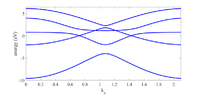
The concept of valence and conduction bands in a five band Hamiltonian refers to the energy levels of electrons in a material. The valence band is the highest energy level that is fully occupied by electrons, while the conduction band is the next highest energy level that is partially filled or empty. These bands play a crucial role in determining the electrical and optical properties of a material.

2. How are the valence and conduction bands related in a five band Hamiltonian?

In a five band Hamiltonian, the valence and conduction bands are related by the energy gap between them. This energy gap is known as the band gap and it determines whether a material is a conductor, insulator, or semiconductor. A larger band gap indicates a wider separation between the valence and conduction bands, making the material less conductive.

3. What factors affect the position of the valence and conduction bands in a five band Hamiltonian?

The position of the valence and conduction bands in a five band Hamiltonian can be influenced by various factors such as the type of material, its crystal structure, and the presence of impurities or defects. Additionally, external factors like temperature, pressure, and electric fields can also affect the position of these bands.

4. How does the band structure of a material affect its properties?

The band structure of a material plays a crucial role in determining its electrical and optical properties. A wider band gap indicates a material with lower conductivity, while a narrower band gap makes a material more conductive. Additionally, the presence of impurities or defects can create energy levels within the band gap, altering the material's properties.

5. What are the applications of understanding valence and conduction bands in a five band Hamiltonian?

Understanding the valence and conduction bands in a five band Hamiltonian is essential for studying the electrical and optical properties of materials. This knowledge is crucial in the design and development of electronic devices such as transistors, solar cells, and LEDs. It also plays a significant role in the field of materials science and can aid in the discovery of new materials with desirable properties.

Similar threads

  • Atomic and Condensed Matter
Replies
4
Views
1K
  • Atomic and Condensed Matter
Replies
11
Views
3K
  • Atomic and Condensed Matter
Replies
7
Views
839
  • Atomic and Condensed Matter
Replies
1
Views
1K
  • Atomic and Condensed Matter
Replies
2
Views
1K
  • Atomic and Condensed Matter
Replies
6
Views
2K
  • Atomic and Condensed Matter
Replies
4
Views
2K
  • Atomic and Condensed Matter
Replies
6
Views
2K
  • Atomic and Condensed Matter
Replies
2
Views
1K
  • Atomic and Condensed Matter
Replies
7
Views
2K
Back
Top