Voltage drop across drain-source for stacked MOSFETs

In summary: It has a drop across it, but it's negligible. In fact, very small amounts of current can flow through a MOSFET even when it's in saturation.
  • #1
jaus tail
615
48
Homework Statement
When three n type mosfets are stacked, what will be potential across V(ds)3 where:
DS1 is drain source of 1st mosfet. Drain is connected to Vdd. Source is connected to drain of second mosfet. Source of second mosfet is connected to third mosfet. Source of third mosfet is connected to resistance that is grounded

Vdd --> Vd1s1 --> Vd2s2 --> Vd3s3 --> R --> Ground
Relevant Equations
Mosfet turns on when Vgs > Vtn and Vds > (Vgs - Vtn)
Here's the circuut:
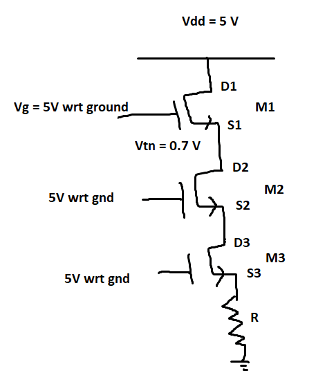
1659082487572.png

Vtn is 0.7 V. So Vs1 (wrt ground) cannot be more than 4.3 V else M1 won't turn on.
Likewise Vs2 and Vs3 (wrt ground) cannot be more than 4.3 V else M2 won't turn on.
So Vs3 = 4.3 V. Even voltage across final resistance is 4.3 V
Assume there's no drop across Mosfet.

But I'm not sure. Will the drop of 0.7 be accumulated. Like Vs3 would be Vdd - 3 times Vtn?
Will Vs3 (wrt ground) be 4.3 V or (5-3 times 0.7) = 2.9 V

The 2 scenarios for this question are:
1) All mosfets are in saturation mode
2) The mosfets can be in linear mode
 
  • Like
Likes Delta2
Physics news on Phys.org
  • #2
Why are all 3 gate voltages equal in this scenario?
jaus tail said:
The 2 scenarios for this question are:
1) All mosfets are in saturation mode
2) The mosfets can be in linear mode
How can you have different situations with the same bias condition?
 
  • Like
Likes jaus tail
  • #3
First, let's assume R >> Rds(on). Rds(on) is the device resistance (drain to source) when it's saturated. This means we don't have to worry about resistive dividers and how much current is flowing.

Second, what you are calling Vtn everyone else calls Vgs(th) (the Gate Source Threshold Voltage). OK, it's somewhat arbitrary what you call things. But... EVERYONE who works with MOSFETs uses Vgs(th), get used to it. Also be suspicious of people who choose a different name, they probably haven't read many MOSFET datasheets, which means they haven't worked in this field much.

OK, now...

Mosfet turns on when Vgs > Vtn ---- Yes.

Mosfet turns on when Vds > (Vgs - Vtn) ---- No. N-MOSFETS can be on even when Vds < 0. This isn't just the built in body diode. They can conduct in either polarity through the channel if Vgs > Vgs(th). This is commonly used in synchronous rectifier circuits to reduce losses since the voltage drop across the channel is (usually) lower than the voltage across the body diode.

Each N-MOSFET is on if Vgs > Vgs(th), it's really that simple. When the MOSFET is on, the drain is essentially connected to the source with a channel resistance of Rds(on), a small value in this case.

So, you have a set of rules (one, really) about when a MOSFET is on. This seems pretty easy to apply in this circuit. Maybe you can think about this and explain again about what is confusing you?
 
  • Like
Likes jaus tail and berkeman
  • #4
DaveE said:
Mosfet turns on when Vgs > Vtn ---- Yes.

Mosfet turns on when Vds > (Vgs - Vtn) ---- No. N-MOSFETS can be on even when Vds < 0. This isn't just the built in body diode. They can conduct in either polarity through the channel if Vgs > Vgs(th). This is commonly used in synchronous rectifier circuits to reduce losses since the voltage drop across the channel is (usually) lower than the voltage across the body diode.

Each N-MOSFET is on if Vgs > Vgs(th), it's really that simple. When the MOSFET is on, the drain is essentially connected to the source with a channel resistance of Rds(on), a small value in this case.

So, you have a set of rules (one, really) about when a MOSFET is on. This seems pretty easy to apply in this circuit. Maybe you can think about this and explain again about what is confusing you?
Ok.. So if Vgs(th) > 0 and if Vds < 0, then also the Mosfet is On, however current direction is reversed. Makes sense.

But assuming that Vgs(th) >0 and all Mosfets are in saturation mode with current flowing from drain to source,
I'm not able to figure out the drop across M1, M2, and M3

The voltage Vd2(wrt ground) and Vd3(wrt ground).

In case of Si Diodes, we take voltage drop as 0.7 and keep on subtracting in series.
Is that the same case here?
berkeman said:
Why are all 3 gate voltages equal in this scenario?

How can you have different situations with the same bias condition?
No, the situations are different. The gate voltages are just sufficient enough to turn on the mosfet as in. Vgs > threshold voltage.

I have no idea how this circuit will work. Electrical engineering is easy with RLC but electronics makes it difficult when diodes and fets come in.
 
  • #5
jaus tail said:
In case of Si Diodes, we take voltage drop as 0.7 and keep on subtracting in series.
Is that the same case here?
No, not for NMOS. A MOSFET in saturation acts just like a resistor.
 
  • Like
Likes jaus tail

1. What is the significance of voltage drop across drain-source for stacked MOSFETs?

The voltage drop across drain-source for stacked MOSFETs is an important parameter that affects the performance and reliability of the device. It determines the amount of current that can flow through the MOSFET and directly impacts its power dissipation and efficiency.

2. How does the number of stacked MOSFETs affect the voltage drop across drain-source?

The number of stacked MOSFETs has a direct impact on the voltage drop across drain-source. As the number of stacked MOSFETs increases, the voltage drop also increases due to the cumulative effect of the individual voltage drops across each MOSFET.

3. What factors can influence the voltage drop across drain-source for stacked MOSFETs?

The voltage drop across drain-source for stacked MOSFETs can be influenced by various factors such as the size and geometry of the MOSFETs, the material used for the MOSFETs, the operating temperature, and the applied voltage.

4. How can the voltage drop across drain-source for stacked MOSFETs be minimized?

To minimize the voltage drop across drain-source for stacked MOSFETs, the design of the MOSFETs can be optimized by reducing their size and improving their geometry. Additionally, using materials with lower resistance and operating at lower temperatures can also help reduce the voltage drop.

5. What are the consequences of a high voltage drop across drain-source for stacked MOSFETs?

A high voltage drop across drain-source for stacked MOSFETs can lead to increased power dissipation, reduced efficiency, and potential device failure. It can also cause overheating and damage to other components in the circuit.

Similar threads

  • Engineering and Comp Sci Homework Help
Replies
0
Views
525
  • Engineering and Comp Sci Homework Help
Replies
20
Views
3K
  • Engineering and Comp Sci Homework Help
Replies
2
Views
1K
  • Engineering and Comp Sci Homework Help
Replies
4
Views
3K
  • Engineering and Comp Sci Homework Help
Replies
1
Views
2K
  • Introductory Physics Homework Help
Replies
3
Views
2K
Replies
4
Views
2K
  • Introductory Physics Homework Help
Replies
2
Views
4K
Replies
4
Views
3K
  • Electrical Engineering
Replies
1
Views
2K
Back
Top