Homework Helper
- 2,076
- 140
Hi everyone. I have seen the design for an NPN Cascode many times, but I want to build a PNP Cascode. I have scoured the internet for a standard design, but to no avail.
The image below is that of a NPN Cascode. I want to create a PNP cascode by flipping things around. I have placed a red line through the circuitry. On the left side of the red line I expect nothing to change when building the PNP Cascode. On the right side of the red line is where I expect things to change.
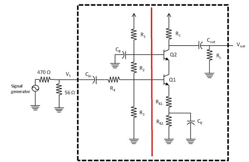
Here is what I am thinking:
1. I will turn transistors ##Q_1## and ##Q_2## into PNP transistors.
2. In the emitter of ##Q_2## there will be no resistor, only the power supply connection ##V_{CC}##.
3. Between the collector of ##Q_2## and the emitter of ##Q_1##, I will place ##R_C## just before the loading circuit. Then I will place the loading circuit.
4. Just after the loading circuit, I will place ##R_{E1}##, ##R_{E2}## and ##C_E##.
5. The collector of ##Q_1## will then be wired to ground.
Does this sound reasonable?
If not, does anyone know what the standard design would look like and could show me?
Thank you.
The image below is that of a NPN Cascode. I want to create a PNP cascode by flipping things around. I have placed a red line through the circuitry. On the left side of the red line I expect nothing to change when building the PNP Cascode. On the right side of the red line is where I expect things to change.
Here is what I am thinking:
1. I will turn transistors ##Q_1## and ##Q_2## into PNP transistors.
2. In the emitter of ##Q_2## there will be no resistor, only the power supply connection ##V_{CC}##.
3. Between the collector of ##Q_2## and the emitter of ##Q_1##, I will place ##R_C## just before the loading circuit. Then I will place the loading circuit.
4. Just after the loading circuit, I will place ##R_{E1}##, ##R_{E2}## and ##C_E##.
5. The collector of ##Q_1## will then be wired to ground.
Does this sound reasonable?
If not, does anyone know what the standard design would look like and could show me?
Thank you.
