CMOS gate for the logic function

Click For Summary
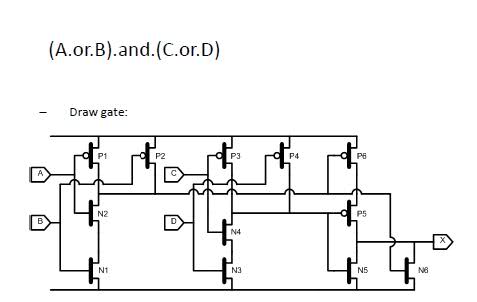
The discussion centers on the logic function (A.or.B).and.(C.or.D) and its representation using CMOS gates. The initial stages involve NAND gates for inputs A, B and C, D, respectively, leading to an output of (A.B)* and (C.D)*. The final stage combines these outputs through a NOR gate, resulting in the expression ( (A.B)* + (C.D)* )*. The conclusion drawn is that the overall circuit indeed represents the intended logic function. The circuit design effectively demonstrates the equivalence of the CMOS implementation to the original logic function.
nobrainer612
Messages
24
Reaction score
0
Hello. One of my friends told me that the logic function for (A.or.B).and.(C.or.D) is
rmidjd.jpg


From a book, I know the P1, P2 , N1, N2 form a NAND. The same for P3, P4, N3, N4.
And P5, P6, N5, N6 form a NOR.

My question is, is this circuit the same as (A.or.B).and.(C.or.D) ?

Thank you
 
Physics news on Phys.org
O/P of first stage(nand) = (A.B)* , second stage = (C.D)*
and third stage(nor) = ( (A.B)* + (C.D)* )* = (A.B)** . (C.D)** = A.B.C.D
 

Similar threads

  • · Replies 1 ·
Replies
1
Views
1K
Replies
1
Views
5K
  • · Replies 2 ·
Replies
2
Views
2K
  • · Replies 7 ·
Replies
7
Views
8K
Replies
9
Views
3K
Replies
2
Views
2K
  • · Replies 4 ·
Replies
4
Views
5K
  • · Replies 2 ·
Replies
2
Views
2K
  • · Replies 14 ·
Replies
14
Views
5K
  • · Replies 14 ·
Replies
14
Views
4K