SUMMARY
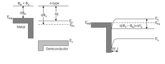
The discussion focuses on the formation of an ohmic contact between a metal and an n-type semiconductor, highlighting the upward bending of the energy bands in the n-type material. This bending occurs due to the accumulation of negative charge within the semiconductor, which creates an electric field that halts further electron flow from the metal. The presence of a non-zero charge density leads to the depletion of electrons from the metal and their accumulation in the semiconductor, resulting in a net negative charge.
PREREQUISITES
- Understanding of semiconductor physics
- Knowledge of n-type semiconductor properties
- Familiarity with energy band theory
- Basic principles of electric fields and charge density
NEXT STEPS
- Research the mechanisms of charge carrier movement in semiconductors
- Explore the concept of energy band bending in p-n junctions
- Learn about ohmic versus Schottky contacts in semiconductor devices
- Investigate the effects of temperature on semiconductor behavior
USEFUL FOR
Electrical engineers, semiconductor physicists, and students studying solid-state electronics will benefit from this discussion, particularly those interested in the behavior of n-type semiconductors and ohmic contacts.
