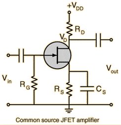
I am familiar with the concept of gate resistance, Rg, in JFET (junction field-effect transistor) amplifier circuits. Rg is a crucial component in these circuits as it controls the input impedance and the gain of the amplifier.
To calculate Rg in a JFET amplifier circuit, we first need to determine the desired input impedance, which is typically set by the manufacturer or the circuit designer. Then, we can use the following formula: Rg = (Vgs / Idss) * (1 - gm * Rl), where Vgs is the gate-source voltage, Idss is the drain-source current at zero gate-source voltage, and gm is the transconductance of the JFET. Rl represents the load resistance connected to the drain of the JFET.
The function of Rg is to provide a controlled resistance between the gate and the source of the JFET, allowing for proper biasing and signal amplification. It also helps to stabilize the amplifier circuit and prevent unwanted oscillations. Additionally, Rg helps to match the input impedance of the JFET with the source signal, ensuring maximum power transfer and minimizing signal distortion.