How Does Gate Resistance Rg Impact JFET Amplifier Performance?

  • Thread starter Thread starter chunhui219
  • Start date Start date
  • Tags Tags
    Gate Resistor
AI Thread Summary
Gate resistance, Rg, is essential in JFET amplifier circuits as it determines input impedance and facilitates proper biasing. It acts as a pull-down resistor, allowing the coupling capacitor to charge and discharge effectively without signal loss. The value of Rg should be significantly larger than the capacitor's reactance at the lowest frequency of interest to ensure signal integrity. Calculating Rg involves considering the desired input impedance and using the formula Rg = (Vgs / Idss) * (1 - gm * Rl). Properly configured, Rg stabilizes the amplifier and enhances performance by matching input impedance and minimizing distortion.
chunhui219
Messages
4
Reaction score
0
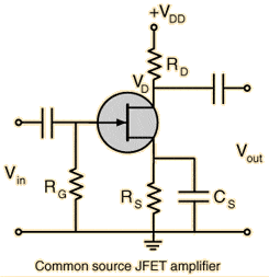
How to calculate gate resistance, Rg in the JFET amplifier circuit?
jfetamp.gif


And What is the function of Rg?
 
Last edited:
Engineering news on Phys.org
Rg is a pull-down resistor and also determines the input impedance of our amplifier.
 
Because the input resistance of the FET itself is very high (many megohms) then the gate resistor is added to allow the coupling capacitor at the input to charge up and discharge in a reasonable time but not fast enough to cause loss of signal.

So, if the input was steady at zero volts and was suddenly increased to 3 volts, the capacitor will pass this change to the gate of the FET because it doesn't (or shouldn't) have time to charge up through the resistor Rg.

But if the input stayed at 3 volts, then the capacitor needs to charge up to 3 volts via Rg so that the voltage across Rg again became zero until any change came along.

The resistor value can be calculated by making it large compared with the reactance of the capacitor at the lowest frequency you want to pass to the gate of the FET.

For example, if the capacitor was 0.01 uF and you wanted to pass a frequency of 300 Hz, the capacitor would have a reactance of 53000 ohms. So, you might make Rg twenty times that, or 1 Megohm.

The capacitor could still charge up in 10 mS, but a 300 Hz signal would have changed polarity several times before that happens.
However, a more permanent change in the input voltage will cause the capacitor to charge up and the voltage on the gate of the FET to return to zero.

If Rg were not there, then the gate of the FET would be dragged to the DC input voltage for many minutes and would probably give no output due to incorrect bias conditions.
 
Thx vk6kro for a brief explanation and Jony130! ! :)


I am familiar with the concept of gate resistance, Rg, in JFET (junction field-effect transistor) amplifier circuits. Rg is a crucial component in these circuits as it controls the input impedance and the gain of the amplifier.

To calculate Rg in a JFET amplifier circuit, we first need to determine the desired input impedance, which is typically set by the manufacturer or the circuit designer. Then, we can use the following formula: Rg = (Vgs / Idss) * (1 - gm * Rl), where Vgs is the gate-source voltage, Idss is the drain-source current at zero gate-source voltage, and gm is the transconductance of the JFET. Rl represents the load resistance connected to the drain of the JFET.

The function of Rg is to provide a controlled resistance between the gate and the source of the JFET, allowing for proper biasing and signal amplification. It also helps to stabilize the amplifier circuit and prevent unwanted oscillations. Additionally, Rg helps to match the input impedance of the JFET with the source signal, ensuring maximum power transfer and minimizing signal distortion.
 
Very basic question. Consider a 3-terminal device with terminals say A,B,C. Kirchhoff Current Law (KCL) and Kirchhoff Voltage Law (KVL) establish two relationships between the 3 currents entering the terminals and the 3 terminal's voltage pairs respectively. So we have 2 equations in 6 unknowns. To proceed further we need two more (independent) equations in order to solve the circuit the 3-terminal device is connected to (basically one treats such a device as an unbalanced two-port...
Thread 'Weird near-field phenomenon I get in my EM simulation'
I recently made a basic simulation of wire antennas and I am not sure if the near field in my simulation is modeled correctly. One of the things that worry me is the fact that sometimes I see in my simulation "movements" in the near field that seems to be faster than the speed of wave propagation I defined (the speed of light in the simulation). Specifically I see "nodes" of low amplitude in the E field that are quickly "emitted" from the antenna and then slow down as they approach the far...
Back
Top