Zrakk
- 7
- 1
Hello,
I'm new and I want to try asking here for any comment or suggestion.
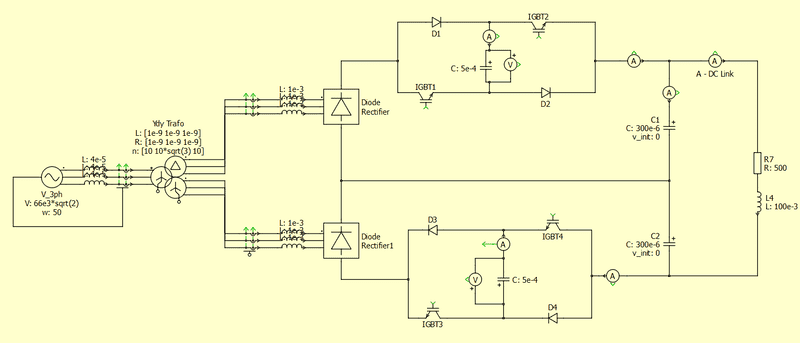
What I have, is a common 12-pulse rectifier with its bridges in series and I included an snubber between DC-link and rectifier output. Is important to note that all inductances before the rectifier are small in order to minimize its impact on this snubber performance. Also, I cleaned the circuit from scopes and control of IGBTs in order to visualize in a better way this system.

The main Idea of this snubber is to give a semi-triangular shape to the current by following a reference (each snubber has it reference which is the same shape but shifted in 30°). The background theory and reason for obtaining this currents, is that doing so, I should have sinusoidal currents at the transformer's primary winding or the AC busbar which is connected this rectifier.
Now, the snubber is supposed to work like this: If output current from snubber is greater than reference, then IGBTs must be turned OFF in order to charge this capacitor and lower output current. Otherwise, if output current is less than reference IGBTs must be turned on, discharging this capacitor and increasing this current. Until now, I can only get this working using DC voltage sources instead of rectifiers (250kV each bridge) as you can see in this picture:

And when using a proper 12-pulse rectifier I get this.

Here the tracking of the reference (green) is really great but for some reason the voltage across the capacitor increases until my simulation crashes. The main idea of this snubber is to turn off both IGBTs when voltage across capacitor is aprox 1V in order to reduce losses while switching, however, if I add that condition in both cases (with DC Voltage Sources and 12-pulse rectifier) the output current from snubber (red) takes a long time to discharge when the snubber have to track the lower sections of this triangular reference.
Any suggestion or recommendation would be truly appreciated as I don't really know what to do instead of changing values of my system without knowing why.
EDIT: I'm using PLECS 3.5.2, if you think something in the logic control should be wrong then I can upload pictures of it too.
I'm new and I want to try asking here for any comment or suggestion.
What I have, is a common 12-pulse rectifier with its bridges in series and I included an snubber between DC-link and rectifier output. Is important to note that all inductances before the rectifier are small in order to minimize its impact on this snubber performance. Also, I cleaned the circuit from scopes and control of IGBTs in order to visualize in a better way this system.
The main Idea of this snubber is to give a semi-triangular shape to the current by following a reference (each snubber has it reference which is the same shape but shifted in 30°). The background theory and reason for obtaining this currents, is that doing so, I should have sinusoidal currents at the transformer's primary winding or the AC busbar which is connected this rectifier.
Now, the snubber is supposed to work like this: If output current from snubber is greater than reference, then IGBTs must be turned OFF in order to charge this capacitor and lower output current. Otherwise, if output current is less than reference IGBTs must be turned on, discharging this capacitor and increasing this current. Until now, I can only get this working using DC voltage sources instead of rectifiers (250kV each bridge) as you can see in this picture:
And when using a proper 12-pulse rectifier I get this.
Here the tracking of the reference (green) is really great but for some reason the voltage across the capacitor increases until my simulation crashes. The main idea of this snubber is to turn off both IGBTs when voltage across capacitor is aprox 1V in order to reduce losses while switching, however, if I add that condition in both cases (with DC Voltage Sources and 12-pulse rectifier) the output current from snubber (red) takes a long time to discharge when the snubber have to track the lower sections of this triangular reference.
Any suggestion or recommendation would be truly appreciated as I don't really know what to do instead of changing values of my system without knowing why.
EDIT: I'm using PLECS 3.5.2, if you think something in the logic control should be wrong then I can upload pictures of it too.

