Location of donor atom electrons in N-type Silicon

In summary, the conversation discusses the energy band diagrams in solid state electronics and the concept of the forbidden gap. It is explained that the region between the top of the valence band and the bottom of the conduction band is known as the forbidden gap, but in N-type semiconductors, the extra electrons from doping atoms create their own energy levels within this gap. This is different from undoped semiconductors, which do not have states in the bandgap. The conversation also mentions a related analogy about putting an apple in a box and how it applies to the concept of the forbidden gap in semiconductors.
  • #1
CoolDude420
198
8
I'm taking a module in solid state electronics and I'm a bit confused with the energy band diagrams. I was told that the region between the top of VB and and the bottom of the CB is the "forbidden gap". However after learning about N-type semiconductors(silicon), I see that the extra electron from the donor atoms have their own energy level right below the bottom of the conduction band in the so called "forbidden gap". How can this be? I'm quite new to solid state and all of its terminology so any help is appreciated.

Heres a pic: [cant post pic]. its the first one on this page
http://hyperphysics.phy-astr.gsu.edu/hbase/solids/dsem.html#c2
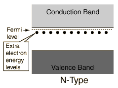
dban2.gif
 
Physics news on Phys.org
  • #2
The states are produced by the doping atoms. Undoped semiconductors don't have states in the bandgap, but doped semiconductors do.
 
  • #3
mfb said:
The states are produced by the doping atoms. Undoped semiconductors don't have states in the bandgap, but doped semiconductors do.

Shouldn't they be in the VB though? Since nothing is meant to be in the Forbidden Gap
 
  • #4
CoolDude420 said:
Since nothing is meant to be in the Forbidden Gap
This statement applies to electrons in undoped semiconductors only. It does not apply to modifications of the crystal.

"I cannot put an apple in a box because there is no box."
"Here I give you a box"
"Now I can put an apple in a box."
 

1. Where are the donor atom electrons located in N-type Silicon?

In N-type Silicon, the donor atom electrons are located in the outermost energy level of the silicon atoms, also known as the valence band.

2. How are the donor atom electrons introduced into N-type Silicon?

The donor atom electrons are introduced into N-type Silicon through a process called doping, where a small amount of impurity atoms, such as phosphorus or arsenic, are purposely added to the silicon crystal structure.

3. Can the location of donor atom electrons in N-type Silicon be changed?

No, the location of donor atom electrons in N-type Silicon cannot be changed after the doping process. The electrons are permanently located in the valence band of the silicon atoms.

4. What is the purpose of having donor atom electrons in N-type Silicon?

The presence of donor atom electrons in N-type Silicon allows for the material to have excess negative charge carriers, making it a good conductor of electricity.

5. How does the location of donor atom electrons affect the properties of N-type Silicon?

The location of donor atom electrons in N-type Silicon greatly affects its electrical conductivity and makes it suitable for use in electronic devices such as transistors and diodes.

Similar threads

  • Atomic and Condensed Matter
Replies
2
Views
2K
Replies
1
Views
1K
  • Atomic and Condensed Matter
Replies
4
Views
1K
Replies
7
Views
1K
  • Atomic and Condensed Matter
Replies
1
Views
2K
Replies
6
Views
2K
  • Atomic and Condensed Matter
Replies
2
Views
2K
  • Atomic and Condensed Matter
Replies
2
Views
2K
  • Advanced Physics Homework Help
Replies
7
Views
1K
  • Electrical Engineering
Replies
1
Views
709
Back
Top