majormajor
- 2
- 0
As an electronic engineer I am not an expert on semiconductor physics but I think I understand the basics of energy band diagrams reasonably well. It all fits together fairly neatly with the normal textbook assumption that we are looking at pure N-type or P-type doping. The problem I have is when they then mention that actually the semiconductor manufacturing process uses predominantly compensation doping, so they might start with a P-type material and then add N-type doping until the material ends up N-type. How exactly this looks on the energy band diagrams is glossed over. There are some fleeting mentions that "oh by the way, the acceptor and donor atoms will neutralize each other".
For example, here's a link from
http://www.doe.carleton.ca/~smcgarry/ELEC3908/Slides/ELEC3908_Lect_3.pdf
Showing the band diagram below for compensation doping:
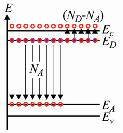
Perhaps I am missing something here but I am baffled as to how the electrons sitting at energy levels very close to the conduction band will now all of a sudden happily fall into the band just above the valence band - especially as the whole story starts with the statement that at room temperature very few electrons have the energy to bridge the 1.1 eV gap for silicon.
To me the logical thing for me to end up with just a mish-mash of "neither p nor n type" silicon, rather then being able to make a usable N-type when we start from P-type.
I would appreciate it if somebody could explain this to me at a qualitative level. If that's at all possible.
For example, here's a link from
http://www.doe.carleton.ca/~smcgarry/ELEC3908/Slides/ELEC3908_Lect_3.pdf
Showing the band diagram below for compensation doping:
Perhaps I am missing something here but I am baffled as to how the electrons sitting at energy levels very close to the conduction band will now all of a sudden happily fall into the band just above the valence band - especially as the whole story starts with the statement that at room temperature very few electrons have the energy to bridge the 1.1 eV gap for silicon.
To me the logical thing for me to end up with just a mish-mash of "neither p nor n type" silicon, rather then being able to make a usable N-type when we start from P-type.
I would appreciate it if somebody could explain this to me at a qualitative level. If that's at all possible.