1msm
- 6
- 0
Hello everyone,
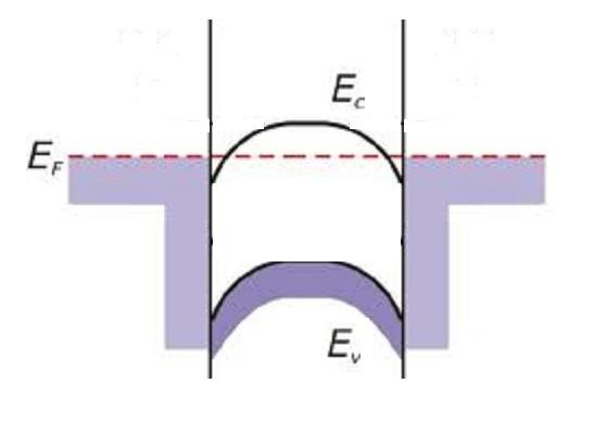
Here i have metal-semiconductor-metal (M-S-M) junctions, p-type semiconductor
separating two similar metals.
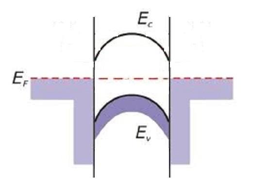
In above picture semiconductor forming schottky barriers with metals, While
in below picture these are ohmic contacts..
If assume that the semiconductor is very thin(few nanometers) and proper biasing
is applied,
Then is it possible for the electrons to tunnel directly from metal to metal..??
Or is there any indirect tunneling paths.?
Any answers would be greatly appreciated!
Here i have metal-semiconductor-metal (M-S-M) junctions, p-type semiconductor
separating two similar metals.
In above picture semiconductor forming schottky barriers with metals, While
in below picture these are ohmic contacts..
If assume that the semiconductor is very thin(few nanometers) and proper biasing
is applied,
Then is it possible for the electrons to tunnel directly from metal to metal..??
Or is there any indirect tunneling paths.?
Any answers would be greatly appreciated!