Purpose of substrate in semiconductor lasers

Click For Summary
SUMMARY

The substrate in semiconductor lasers serves multiple critical functions, including acting as one of the electrodes, facilitating the epitaxial growth of active layers, and enabling local doping through techniques like ion implantation. Additionally, the substrate can function as a heat sink and allows for the simultaneous production of numerous small devices, ensuring structural integrity and connectivity. Common substrate materials include Silicon, particularly in applications like NAND flash memory, where doping is utilized to achieve desired electrical properties.

PREREQUISITES
  • Understanding of semiconductor physics
  • Familiarity with epitaxial growth techniques
  • Knowledge of ion implantation processes
  • Basic concepts of electrical doping in semiconductors
NEXT STEPS
  • Research epitaxial growth methods for semiconductor layers
  • Learn about ion implantation techniques in semiconductor manufacturing
  • Explore the role of substrates in thermal management of electronic devices
  • Study the properties and applications of Silicon in semiconductor technology
USEFUL FOR

Electrical engineers, semiconductor researchers, and professionals involved in the design and manufacturing of electronic devices, particularly those focusing on semiconductor lasers and related technologies.
Goodver
Messages
101
Reaction score
1
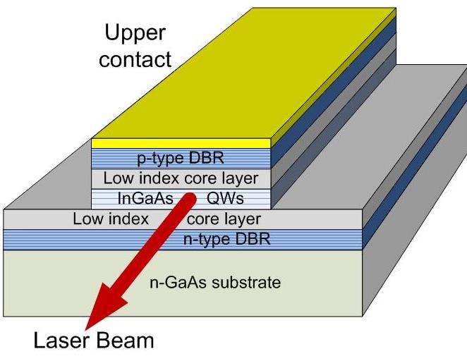
What is a purpose of a substrate in an electronic device? In particular semiconductor lasers, why is it made of semiconductor?

Thank you.

BRW_Laser_Sctruc.jpg
 
Last edited:
Physics news on Phys.org
In many cases the substrate is one of the electrodes. Otherwise it is chosen because the active layers can be easily grown epitaxially on the substrate material, or because the active components can be produced by locally doping the substrate, e.g. by ion implantation. Sometimes the substrate acts as a heat sink. Last but not least, simultaneously producing a large number of tiny devices on a common substrate is a neat way of holding everything together and connected.

I'm sure I forgot some other good reasons.
 
  • Like
Likes   Reactions: Goodver
I think M Quack covered it pretty well. For example, look at MOSFETs - very tiny transistors. The "substrate" is often Silicon for things like NAND flash memory, and areas of it are either n or p type doped for various reasons that you can look up.
 

Similar threads

  • · Replies 5 ·
Replies
5
Views
2K
  • · Replies 2 ·
Replies
2
Views
2K
  • · Replies 1 ·
Replies
1
Views
2K
  • · Replies 1 ·
Replies
1
Views
9K
  • · Replies 2 ·
Replies
2
Views
3K
  • · Replies 1 ·
Replies
1
Views
1K
  • · Replies 10 ·
Replies
10
Views
2K
  • · Replies 8 ·
Replies
8
Views
2K
  • · Replies 1 ·
Replies
1
Views
2K
  • · Replies 3 ·
Replies
3
Views
2K