Simulating this cascoded NMOS logic circuit

  • Context: Engineering 
  • Thread starter Thread starter elektro2021
  • Start date Start date
  • Tags Tags
    Circuit Logic
Click For Summary

Discussion Overview

The discussion revolves around simulating a cascoded NMOS logic circuit as part of an exercise from Rabaey's "Digital Integrated Circuits: A Design Perspective." Participants are focused on achieving a specific delay of 100 ps while driving a 100 fF load, using 0.25 μm devices. The conversation includes aspects of circuit sizing, logic function identification, and simulation approaches.

Discussion Character

  • Homework-related
  • Technical explanation
  • Exploratory
  • Debate/contested

Main Points Raised

  • One participant seeks assistance in sizing and simulating a specific NMOS logic circuit to achieve a 100 ps delay.
  • Another participant questions whether the logic function with complementary outputs has been identified and how the simulation will be conducted.
  • Clarification is requested regarding a symbol in the circuit, which is identified as a memory element or "keeper" circuit that prevents floating inputs.
  • A participant expresses a desire to size the NMOS transistors by hand rather than using a simulator, aiming for a specific delay while driving a load.
  • There is a suggestion to compute the current charge/discharge for the 100 fF capacitor, with a proposed formula involving voltage change over time.
  • Participants discuss the relationship between NMOS current and the aspect ratio (W/L) of the transistors, with one expressing uncertainty about how to proceed.
  • Another participant prompts for insights from class notes regarding aspect ratio effects on voltages and currents.

Areas of Agreement / Disagreement

Participants have not reached a consensus on the approach to sizing the NMOS transistors or the identification of the logic function. Multiple viewpoints and methods are being explored, and the discussion remains unresolved.

Contextual Notes

Participants have not provided complete details on their calculations or assumptions regarding the circuit parameters, and there are unresolved questions about the logic function and simulation methods.

elektro2021
Messages
6
Reaction score
0
New poster has been reminded to always show their work when starting schoolwork threads
Homework Statement
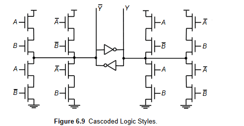
Size and simulate the circuit (IMAGE BELOW) so that it achieves a 100 ps delay (50-50) using 0.25 μm devices, while driving a 100 fF load on both differential outputs. (VDD = 2.5V) Assume A, B and their complements are available as inputs.
Relevant Equations
vailable common data for nmos are following Vt=0.43(V),Vdsat=0.63(V),k'=115x10^-6 (A/V^2),lambda=0.06(v^-1)
I need help for following exercise from Rabaey - Digital Integrated Circuits: A Design Perspective

Size and simulate the circuit (IMAGE BELOW) so that it achieves a 100 ps delay (50-50) using 0.25 μm devices, while driving a 100 fF load on both differential outputs. (VDD = 2.5V) Assume A, B and their complements are available as inputs.
Available common data for nmos are following Vt=0.43(V),Vdsat=0.63(V),k'=115x10^-6 (A/V^2),lambda=0.06(v^-1)
Please help me.
2022-02-04_100733.png
 
Physics news on Phys.org
Welcome to PF.
Have you yet identified the two input logic function with a complementary output ?
How will you simulate the gate and delay ?
 
Welcome to PF. :smile:

You need to show some effort before we can provide tutorial help. Please show us how you will approach this question.

Also, I'm a little confused by this symbol in the middle of your NMOS logic circuit -- what is it meant to represent? Is it some IP that is defined elsewhere in the problem statement?

1644244984698.png
 
berkeman said:
Also, I'm a little confused by this symbol in the middle of your NMOS logic circuit
It is a memory element made from two soft output inverters.
It retains the last valid state of the gate, so prevents floating inputs consuming current.
 
  • Informative
Likes   Reactions: berkeman
Ah, it's a "keeper" circuit. Got it, thanks @Baluncore :smile:
 
Baluncore said:
Welcome to PF.
Have you yet identified the two input logic function with a complementary output ?
How will you simulate the gate and delay ?
I think it's a XOR port for Y and XNOR for Y negate.I don't want to simulate the circuit by a simulator but I want to size (by hand) W/L for NMOS transistors to get a 100 ps delay (50-50) using 0.25 μm devices, while driving a 100 fF load on both differential outputs.
 
elektro2021 said:
I don't want to simulate the circuit by a simulator but I want to size (by hand) W/L for NMOS transistors to get a 100 ps delay (50-50) using 0.25 μm devices, while driving a 100 fF load on both differential outputs.
Okay, can you show us how you are going to approach that?
 
elektro2021 said:
I want to size (by hand)
Have you attempted to do that yet?
 
I think that I need to compute current charge/discharge for 100 fF capacitor...what do you think?
 
  • #10
Any help?
 
  • #11
elektro2021 said:
Any help?
You go first... :wink:
 
  • #12
I think that Ic=C*(dv/dt) con C=100 fF and dv/dt= (VDD/2)/T con T=100ps and VDD=2.5V...what do you think?
 
  • #13
So after you determine the voltages and currents involved, how will you choose the aspect ratio for your geometry?

elektro2021 said:
I want to size (by hand) W/L for NMOS transistors to get a 100 ps delay (50-50) using 0.25 μm devices
 
  • #14
I don't know...I think that NMOS current depends by W/L...please help me
 
  • #15
We *are* trying to help. What do your class notes say about aspect ratio effects on voltages and currents?
 

Similar threads

  • · Replies 1 ·
Replies
1
Views
2K
  • · Replies 4 ·
Replies
4
Views
4K
  • · Replies 1 ·
Replies
1
Views
2K
  • · Replies 1 ·
Replies
1
Views
15K