Sketch Vin-Vout in MOS transistor

  • Thread starter Thread starter anhnha
  • Start date Start date
  • Tags Tags
    Sketch Transistor
Join the discussion
Registration is free. Ask a follow-up in this thread, or start your own.
1 reply · 5K views
anhnha
Messages
179
Reaction score
1
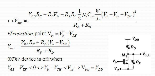
Can you help me check my work and tell me what is the application of the circuit?

Homework Statement


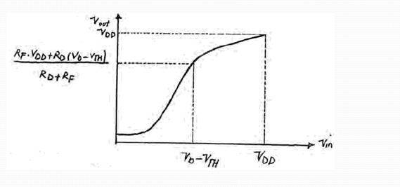
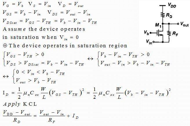
Sketch Vout versus Vin as Vin varies from 0 to VDD. Identify important points.


Homework Equations


MOS transistor equations in triode and saturation modes.
The Attempt at a Solution


attachment.php?attachmentid=59640&stc=1&d=1371488951.jpg

attachment.php?attachmentid=59641&stc=1&d=1371488951.jpg

attachment.php?attachmentid=59642&stc=1&d=1371488951.jpg
 

Attachments

  • 3.15_1.JPG
    3.15_1.JPG
    39.1 KB · Views: 1,461
  • 3.15_2.JPG
    3.15_2.JPG
    25.3 KB · Views: 1,105
  • 3.15_3.JPG
    3.15_3.JPG
    10.9 KB · Views: 1,597
Physics news on Phys.org
I'm not going to check your math but I can tell you that this configuration is known as the common-gate configuration, analogous to the common-base mode of a BJT.

EDIT: the purpose is to improve frequency response by eliminating the so-called "Miller effect". Put a small capacitance Cgd in the common-source configuration & you will see this. The price is a lower input impedance.

Adding Rf reduces the gain ∂Vout/∂Vin but it does linearize it somewhat (for low values of -Vin, or in cutoff mode, ∂Vout/∂Vin = R/Rf where R = Rd||Rf.
 
Last edited: