Variable Gain Preamplifier using dc control voltage

  • Thread starter Thread starter nauman
  • Start date Start date
Click For Summary
SUMMARY

The forum discussion focuses on simulating a variable gain preamplifier for an acoustic hydrophone operating between 90KHz and 110KHz using Orcad Capture. The main issue raised is that the output remains zero regardless of the DC control voltage applied to the base of the Q04 transistor. Participants suggest that the problem may stem from the simulation model rather than the circuit design, with specific recommendations to verify transformer connections and grounding issues in Orcad PSpice. Successful simulation results were achieved using LTspice with BC547 transistors, indicating that the gain can be adjusted from 5 to 18 based on the control voltage.

PREREQUISITES
  • Understanding of variable gain amplifiers and their applications
  • Familiarity with Orcad Capture and PSpice simulation tools
  • Knowledge of transistor operation, specifically BC547 characteristics
  • Basic principles of transformer operation and impedance matching
NEXT STEPS
  • Investigate transformer simulation techniques in Orcad PSpice
  • Learn about troubleshooting floating nodes in circuit simulations
  • Explore the use of LTspice for simulating variable gain amplifiers
  • Review best practices for schematic design to avoid connection errors
USEFUL FOR

Electronics engineers, circuit designers, and students working on amplifier simulations, particularly those using Orcad Capture and PSpice for acoustic applications.

nauman
Messages
98
Reaction score
5
TL;DR
Orcad Capture simulatin of transistors based Variable Gain Preamplifier is not working properly
Hi all

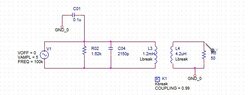
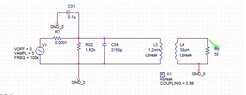
I am trying to simulate input stage of a variable gain preamplifier for acoustic hydrophone operating in frequency range of 90KHz to 110KHz. It is transistor based preamplifier. The gain of preamplifier (Q01) is controlled through dc control voltage (Vc) connected with base of Q04 transistor through R05. I have attached the Orcad Capture Schematic snapshot.

The problem is that whatever dc control i set, output is still zero!

Any help in this regard is much appreciated.

Preamp Input Stage Schematics.jpg
 
Engineering news on Phys.org
Is ##V_C## connected backwards? Also, what is the purpose of ##R_{03}##? I'm not understanding that part of the bias circuit...

EDIT/ADD -- Where did you get this circuit from?
 
OK, I haven't really solved this circuit. It basically looks ok. But here are my impressions based on a bunch of quick calculations with big approximations and maybe errors:
1) The DC bias looks ok at about 4mA.
2) The first stage gain of R02⋅Ie/Vt is about 260. So 260mV into the tank output filter. I would expect something like 4 to 8V at the output.
3) The LC tank output filter looks OK at 100KHz and Q=2. The load isn't significant compared to R02 or Zc, but see the next comment. I'm assuming the transformer steps the voltage up, not down.
4) Is your transformer backwards? I'm not sure about the ORCAD notation, but if the magnetizing inductance is 1.2mH seen from the left side and 4.2uH from the right, that's a turns ratio of 17:1, right?

Have you verified the simulator measurements of internal stuff with "rule of thumb" analysis? You say the signal is zero. Where is it zero? Which voltages and/or currents?

Maybe @Baluncore can set us straight. He's good at this and usually works harder than us.
 
  • Like
Likes   Reactions: Baluncore
nauman said:
The problem is that whatever dc control i set, output is still zero!
I think you have a modelling problem, not a circuit problem.
Simulation works in LTspice using 2x BC547.
Voltage gain is adjustable from 5 to 18, as Vc goes from -8.0 to -0.5 volt.

Transformer is matching Q1 collector load of 1k62 to 50R output.
Zratio = 1k62 / 50R = 32.4 down.

Var-Gain-Pre-Amp-0.png
 

Attachments

  • Like
Likes   Reactions: DaveE
Baluncore said:
I think you have a modelling problem, not a circuit problem.
Thanks very much for help. I think you are right. I have problem in simulating the transformer in Orcad Capture as i am trying to simulate filter circuit connected with Q01 collector standalone and have following errors!
"ERROR -- Node N27120 is floating
ERROR -- Node N27066 is floating
ERROR -- Voltage source and/or inductor loop involving V_V1
You may break the loop by adding a series resistance"
Have you any experience with transfrmers simulations in Orcad Pspice?
 

Attachments

  • Filter_Circuit.jpg
    Filter_Circuit.jpg
    16.3 KB · Views: 29
Sorry, but no experience in the last 25 years with Orcad.

Spice simulators have a steep learning curve, which sometimes overhangs the climber.
I guess you have GND_0 floating because it is not grounded to ground node 0 of the simulation.
 
nauman said:
Have you any experience with transfrmers simulations in Orcad Pspice?
30 years ago I used PSpice a lot, LOL. Any knowledge there was lost long ago.
Like Baluncore, I'm an LTSpice convert. But really, I'm not a big fan of simulators for circuits that can be done by hand. Granted, you're stupid if you don't check with a simulator at some point. But they aren't great for design or understanding, you just get results.
 
Last edited:
Anyway, I think your next step is to either start deleting things, or build the circuit up bit by bit. Get rid of the transformer and see if that helps. The whole Q4 network can be replaced with a current source...
 
Also, recheck all of your trace junctions. I used to dislike ORCAD because traces don't (didn't) automatically connect. Maybe follow the old Mil-Spec rule that schematics should never have junctions where 4 (or more) traces connect. Then you only have crossings (not connected) and tees (connected). It makes it easy to check visually and (bonus! If you're a time traveler) is compatible with old crappy copiers and blueprint machines.
 
  • #10
Baluncore said:
I guess you have GND_0 floating because it is not grounded to ground node 0 of the simulation.
I am able to simulate by adding a small resistance in series with source V1 and grounding the source but still output is not correct i.e. 1mVpp across 50 ohm load whereas it should be around 800mVpp!
 

Attachments

  • Filter_Circuit2.jpg
    Filter_Circuit2.jpg
    17.2 KB · Views: 26

Similar threads

  • · Replies 12 ·
Replies
12
Views
4K
Replies
7
Views
2K
Replies
26
Views
7K
  • · Replies 24 ·
Replies
24
Views
4K
  • · Replies 3 ·
Replies
3
Views
4K
  • · Replies 8 ·
Replies
8
Views
3K
  • · Replies 22 ·
Replies
22
Views
4K
  • · Replies 5 ·
Replies
5
Views
5K
  • · Replies 13 ·
Replies
13
Views
6K
  • · Replies 5 ·
Replies
5
Views
3K