Voltage Multiplier: Why Don't Current Divide Between Diodes?

Click For Summary
SUMMARY

The discussion centers on the operation of voltage multipliers, specifically negative voltage triplers and quadrouplers, utilizing diodes D1, D2, D3, and D4. It is established that current does not divide between the diodes due to the impedance differences in the paths, with current favoring the route through fewer capacitors. Capacitors C1 and C3 serve as coupling capacitors, while C2 and C4 act as smoothing capacitors. The output voltage across C4 is confirmed to be four times the pulse amplitude minus four diode drops, validating the circuit's function as a negative voltage quadrupler.

PREREQUISITES
  • Understanding of diode behavior in circuits
  • Knowledge of capacitor functions in voltage multipliers
  • Familiarity with AC sine wave characteristics
  • Basic principles of impedance and reactance in electrical circuits
NEXT STEPS
  • Study the operation of voltage multipliers using ideal diodes
  • Learn about the role of capacitors in smoothing and coupling applications
  • Explore simulations of voltage multipliers with different input waveforms
  • Investigate the differences between negative voltage doublers and quadrouplers
USEFUL FOR

Electrical engineers, circuit designers, and students studying power electronics who seek to understand the principles of voltage multiplication and diode behavior in AC circuits.

Hassan Raafat
Messages
37
Reaction score
5
in Voltage Tripler and Quadrupler , why don't current divide between two diodes ( D1 , D3 ) or ( D2 , D4 ) ?
they are forward in the same cycle , right ?
I understand that charging happens in a very little time , so two cycles already is not shown on oscilloscope but in BoyleStad is explained that in every half cycles (in the first two) one diode only works ...
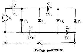
upload_2016-4-8_17-49-43.jpeg
 
Engineering news on Phys.org
Hassan Raafat said:
in Voltage Tripler and Quadrupler , why don't current divide between two diodes ( D1 , D3 ) or ( D2 , D4 ) ?
they are forward in the same cycle , right ?
I understand that charging happens in a very little time , so two cycles already is not shown on oscilloscope but in BoyleStad is explained that in every half cycles (in the first two) one diode only works ...
View attachment 98799
I am no expert but here's what I think..
Assume the diodes are ideal. Current flows through C1 and D1 because this path offers less impedance than C1-C3-D2-C2 path. There are three caps in the second path, hence reactance offered is more. Also, when D1 turns on, it shorts out C2, D2 and C3.
 
  • Like
Likes   Reactions: Hassan Raafat
This is a negative voltage quadrupler.
  • C2 and C4 are smoothing capacitors, storing energy between pulses
  • C1 and C3 are coupling capacitors, connecting the pulses from Vi to the diode junctions.
Now look at the capacitor/diode combinations: C1/D1 rectifies the negative peak pulse voltage and stores it on C1. The pulses are still present, but they are now referred to the voltage across C1. The same argument goes for C3/D3, except that the voltage across C2 is added to the rectified voltage across C3.

In the same way, the negative pulse is rectified across D2 and stored in C2. The resulting voltage across C2 is the sum of the voltage across C1 and the negative pulse amplitude. Finally, The negative pulse is also rectified across D4 and stored in C4. The resulting voltage across C4 is the sum of the voltage across C3 and the negative pulse amplitude. All in all - the voltage on C4 is 4 times the pulse amplitude minus 4 diode drops.
 
  • Like
Likes   Reactions: Hassan Raafat
Svein said:
This is a negative voltage quadrupler.
  • C2 and C4 are smoothing capacitors, storing energy between pulses
  • C1 and C3 are coupling capacitors, connecting the pulses from Vi to the diode junctions.
Now look at the capacitor/diode combinations: C1/D1 rectifies the negative peak pulse voltage and stores it on C1. The pulses are still present, but they are now referred to the voltage across C1. The same argument goes for C3/D3, except that the voltage across C2 is added to the rectified voltage across C3.

In the same way, the negative pulse is rectified across D2 and stored in C2. The resulting voltage across C2 is the sum of the voltage across C1 and the negative pulse amplitude. Finally, The negative pulse is also rectified across D4 and stored in C4. The resulting voltage across C4 is the sum of the voltage across C3 and the negative pulse amplitude. All in all - the voltage on C4 is 4 times the pulse amplitude minus 4 diode drops.
I think that your last sentence is confusing me , C4 has 2 times and also C2 has 2 times so when I took the voltage on the bottom from right to left I have 4Vs - 4 Diode drops
 
cnh1995 said:
I am no expert but here's what I think..
Assume the diodes are ideal. Current flows through C1 and D1 because this path offers less impedance than C1-C3-D2-C2 path. There are three caps in the second path, hence reactance offered is more. Also, when D1 turns on, it shorts out C2, D2 and C3.
If I understood u well , u mean that current will choose the shortest path to pass through (assuming all diodes are ideal) and so to have less capacitors in the path to have less impedance , right ?
 
Hassan Raafat said:
If I understood u well , u mean that current will choose the shortest path to pass through (assuming all diodes are ideal) and so to have less capacitors in the path to have less impedance , right ?
If D1 is turned on, it will short out D3, C3 and C2. So, D3 won't conduct. If D3 were on, then surely there would be some voltage drop across C3 which means D1 would also be on. But, if D1 is on, D3 can't be on. So, D3 is off in the first half cycle.
 
  • Like
Likes   Reactions: Hassan Raafat
Svein said:
This is a negative voltage quadrupler.
  • C2 and C4 are smoothing capacitors, storing energy between pulses
  • C1 and C3 are coupling capacitors, connecting the pulses from Vi to the diode junctions.
Now look at the capacitor/diode combinations: C1/D1 rectifies the negative peak pulse voltage and stores it on C1. The pulses are still present, but they are now referred to the voltage across C1. The same argument goes for C3/D3, except that the voltage across C2 is added to the rectified voltage across C3.

In the same way, the negative pulse is rectified across D2 and stored in C2. The resulting voltage across C2 is the sum of the voltage across C1 and the negative pulse amplitude. Finally, The negative pulse is also rectified across D4 and stored in C4. The resulting voltage across C4 is the sum of the voltage across C3 and the negative pulse amplitude. All in all - the voltage on C4 is 4 times the pulse amplitude minus 4 diode drops.
Sorry, several incorrect statements:
  1. It is a negative voltage doubler.
  2. The statements regarding the capacitors are correct.
This is a simulation of the circuit. The blue trace is the output of the pulse generator. The red trace is the voltage across D1. The green trace is the voltage at the output (junction D4/C4).
upload_2016-4-10_7-37-35.png
 
  • Like
Likes   Reactions: Hassan Raafat
It is certainly more than a doubler. The actual measured output may not be quadruple of the peak voltage but in any textbook I have seen this would be more than just a doubler.
 
  • Like
Likes   Reactions: Hassan Raafat
Averagesupernova said:
It is certainly more than a doubler. The actual measured output may not be quadruple of the peak voltage but in any textbook I have seen this would be more than just a doubler.
Oops - we are talking about two different things here. I am used to thinking about generating a voltage from a pulse train - and then the circuit doubles the pulse amplitude. But if you are talking about a sine wave AC input, the circuit quadruples the sine wave amplitude (the sine wave amplitude is half the peak-to-peak voltage).
 
  • Like
Likes   Reactions: Hassan Raafat
  • #10
Svein said:
if you are talking about a sine wave AC input, the circuit quadruples the sine wave amplitude (the sine wave amplitude is half the peak-to-peak voltage).
upload_2016-4-11_5-58-56.png

Here is a simulation with a 5V amplitude sine wave at the input. The output is then 4 times the amplitude (and 2 times the p-p voltage).
 
  • Like
Likes   Reactions: Hassan Raafat
  • #11
There really is no difference. It's just how the input is spec'd. An AC voltage that is typically driving a voltage multiplier in a power supply is always spec'd as RMS. The attachment in post #7 is no different. Typically we don't spec 0 to 5 volt 50% duty cycle waveform as 2.5 volt RMS but it still multiplies it in the same manner.
 
  • Like
Likes   Reactions: Hassan Raafat
  • #12
Svein said:
View attachment 98925
Here is a simulation with a 5V amplitude sine wave at the input. The output is then 4 times the amplitude (and 2 times the p-p voltage).
Thanks a lot , this images really helped me to understand it ... I'm grateful for that my professor :smile:
 

Similar threads

  • · Replies 14 ·
Replies
14
Views
2K
  • · Replies 6 ·
Replies
6
Views
3K
  • · Replies 10 ·
Replies
10
Views
3K
  • · Replies 5 ·
Replies
5
Views
4K
  • · Replies 26 ·
Replies
26
Views
4K
Replies
5
Views
3K
  • · Replies 2 ·
Replies
2
Views
2K
  • · Replies 6 ·
Replies
6
Views
3K
  • · Replies 37 ·
2
Replies
37
Views
8K
  • · Replies 3 ·
Replies
3
Views
3K