Why Does My BJT Simulation Show Different Collector Current Than Calculated?

  • Thread starter whatsap45
  • Start date
  • Tags
    Bjt
In summary, The speaker is having trouble calculating the correct IC current in a circuit, despite applying KCL and using the correct formula. They are using the equation Ic=βIb with a β value of 175, but are getting a significantly higher current than expected. They are also unsure how to explain the reason for the collector-emitter voltage being approximately zero when there is a current at the base. They are operating the transistor in a non-linear region and it is suggested that the transistor may be driven into saturation, resulting in a zero voltage across R1 and a corresponding zero current.
  • #1
whatsap45
5
0
1. As compared to the circuit as shown in the figure, i applied KCL in the circuit and still couldn't get the right Ic current at the collector as shown in the simulation.
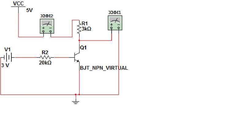
Untitled.jpg


2. The IC current for XMM2 is 1.64mA but i got 22.12mA instead in my calculation. (I'm using the Ic=βIb where β=175 for the solution.)


3. Ib= Vcc-Vbe/20k Ib=3-0.7/20k Ib=0.115mA Ic=Ib (175) Ic=22.12mA

Any idea? Somehow, i need to explain it in my discussion for my report. I screwed up with the calculation and i have no idea of explaining the reason why Vce is approximately equal to 0 when there is a Ib current due to Vb voltage at its base.

More info, XMM1 shows the voltage of 77.205mV...
 
Physics news on Phys.org
  • #2
You're operating the transistor in a non-linear region. Ic will not be β*Ib there.

Suppose that the transistor was driven into saturation (turned on as hard as it can go). Then the collector-emitter voltage would be just about zero (looks like an "ON" switch). What would be the voltage across R1? What then its current?
 

FAQ: Why Does My BJT Simulation Show Different Collector Current Than Calculated?

What is a BJT?

A BJT, or bipolar junction transistor, is a type of semiconductor device used in electronic circuits to amplify or switch signals. It is composed of three layers of doped silicon material, forming two PN junctions.

Why am I unable to solve this simple BJT question?

There could be several reasons for this. It could be due to a lack of understanding of BJT fundamentals, incorrect application of BJT equations, or a mistake in the problem statement itself. It is important to review the basics and carefully analyze the problem before attempting to solve it.

What are the key parameters of a BJT?

The key parameters of a BJT are the collector current (IC), base current (IB), and emitter current (IE). The ratio of collector current to base current (β) and the ratio of collector current to emitter current (α) are also important parameters to consider.

How do I solve a BJT circuit?

To solve a BJT circuit, you need to first determine the operating mode of the transistor (active, cutoff, or saturation), then use the appropriate equations and circuit analysis techniques to find the values of the key parameters. It is important to follow a systematic approach and double-check your calculations to ensure accuracy.

Where can I find resources to learn more about BJTs?

There are many online resources available, such as textbooks, tutorials, and video lectures, that can help you learn more about BJTs. You can also consult with experienced engineers or attend workshops and seminars to enhance your understanding of this topic.

Similar threads

Replies
8
Views
2K
Replies
4
Views
2K
Replies
2
Views
2K
Replies
7
Views
5K
Replies
1
Views
2K
Replies
16
Views
3K
Replies
2
Views
3K
Back
Top