Research which involves some semiconductors

In summary, semiconductors can be classified as intrinsic or extrinsic, with extrinsic further divided into n-type and p-type. The addition of an impurity in a semiconductor creates extrinsic semiconductors, with the excess electrons or holes living in dopant levels near the conduction or valence band. The energy levels introduced by doping atoms are usually quite close to the band edges and will be completely ionized, meaning they cannot contribute to optical excitations. One reason for doping semiconductors is to create built-in electric fields, which can be used in devices such as photodiodes and solar cells. Changing the doping level or type can change the band structure and thus the properties of the semiconductor.
  • #1
Shadowz
43
0
Hi everyone,

Recently I am working with a research which involves some semiconductors. In the basic level, semiconductor can be classified as intrinsic (undoped) and extrinsic (doped) semiconductor. Then extrinsic semiconductor can be divided into n-type and p-type. For example, the below figure illustrates the n-type semiconductor.
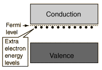
nsem2.gif


According to my understanding, since semiconductors have large band-gap (not as large as insulator) so that electrons cannot move easily from valence band to conduction band, and that's why people add an additional element to the semiconductor to make them become extrinsic semiconductor. Thus, I expected the extra electrons (for n-type) will move from the extra energy level (as seen in the above figure) to the conduction band and the valence band will not involve in this excitation.

However, as I read more and more about semiconductor and electrochemistry, a lot of authors draw n-type and p-type semiconductors in which electrons move from valence band to conduction band

This is a figure I got from wiki
200px-N-Type_Semiconductor_Bands.svg.png

Even though this picture is not great, it represents the idea that for extrinsic semiconductor, electrons move from valence band to conduction band (but if it's true then why they have to add impurities to the intrinsic semicondutor).

Any explanations or suggestions would be great helps for me.


Thanks.
 

Attachments

  • nsem2.gif
    nsem2.gif
    3 KB · Views: 505
Physics news on Phys.org
  • #2


I don't see how the second picture represents the idea that electrons move directly from valence to conduction band. All it shows is there are more electrons in the conduction band than holes in the valence band, due to n-doping. It seems that they neglected to draw the energy level of the donor atoms.

Is there a source somewhere which states that electrons jump from valence to conduction band more easily when the semiconductor is doped?
 
  • #3


As explained above, the excess electrons live in dopant levels near the conduction band. They are not caused by exciting valence electrons. The "[itex]\mathbf{E \uparrow}[/itex]" in the picture represents the energy axis, not an excitation process.
 
  • #4
So, if I consider an intrinsic semiconductor A, I have to supply a optical energy E = E band-gap to excite electrons from valence band to conduction band.

Now, if I add an additional element to make A become extrinsic semiconductor, then the optical energy I need to supply will be less than E, right?

Furthermore, if A is a n-type semiconductor, then the electrons in the valence band will have no or little contribution in the conductivity of the material, right?

However, the book I read draw the n-type semiconductor as seen in the below figure
http://i31.photobucket.com/albums/c385/Thanh_Do/1-10.jpg
The caption of the picture, based on the book is "The effect of illumination at an ideal n-type semiconductor-electrolyte interface"So I don't understand the picture.Thanks
 
  • #5
Shadowz said:
So, if I consider an intrinsic semiconductor A, I have to supply a optical energy E = E band-gap to excite electrons from valence band to conduction band.

Now, if I add an additional element to make A become extrinsic semiconductor, then the optical energy I need to supply will be less than E, right?

Furthermore, if A is a n-type semiconductor, then the electrons in the valence band will have no or little contribution in the conductivity of the material, right?
The donor atoms are ionized by thermal excitation. I don't remember if optical illumination helps to ionise them, but I suppose it should. Someone ought to confirm this.

Shadowz said:
However, the book I read draw the n-type semiconductor as seen in the below figure
http://i31.photobucket.com/albums/c385/Thanh_Do/1-10.jpg
The caption of the picture, based on the book is "The effect of illumination at an ideal n-type semiconductor-electrolyte interface"
This depends on the frequency of the light shone on the semiconductor. If it's high-freqency light, then of course a lot of valence electrons would be excited across the band-gap, which overwhelms and makes almost negligible the contibution to electrical conductivity by the donor electrons. At this point, when this happens the semiconductor behaves intrinsically, just as an extrinsic semiconductor would behave intrinsically (in terms of electrical conductivity) at high temperatures.
 
  • #6


Defennder said:
This depends on the frequency of the light shone on the semiconductor. If it's high-freqency light, then of course a lot of valence electrons would be excited across the band-gap, which overwhelms and makes almost negligible the contibution to electrical conductivity by the donor electrons. At this point, when this happens the semiconductor behaves intrinsically, just as an extrinsic semiconductor would behave intrinsically (in terms of electrical conductivity) at high temperatures.

Thank you.

But if it's so then why don't people just use intrinsic semiconductor instead of using an extrinsic semiconductor and have it behave intrinsically?
 
  • #7


There may be other parameters that they care for besides the band gap (carrier concentration, mobility, etc.).
 
  • #8


So you don't always have to use high-frequency light or place the semiconductor under high-temperatures just to increase its electrical conductivity. Extrinsic semiconductors have other properties which are also used in a lot of other electronic devices such as diodes, FETs and transistors.
 
  • #9


Gokul43201 said:
There may be other parameters that they care for besides the band gap (carrier concentration, mobility, etc.).

Can you talk a little bit more about this please?
 
  • #10


In most applications the energy levels introduced by the doping atoms will be quite close to the band edges and will be completely ionized (that is, donors have yielded an electron to the conduction band and acceptors have accepted an electron from the valence band leaving a hole). In this regime the impurity levels cannot contribute in optical excitations as they are already ionized (no electron left to excite). Opitcal excitation usually occurs between the valence band and the conduction band.

One reason for doping semiconductors before optical excitation is to create built-in electric fields, e.g. a pn-junction. When an electron-hole pair is created in the pn-junction the electric field separates these, creating a voltage. This is the principle behind a photodiode (or solar cell)

In the figure you are referring to (http://i31.photobucket.com/albums/c3...nh_Do/1-10.jpg ) there is bending of the energy bands which represents the presence of an electric field. This field will sweep the electron and hole to either side generating a voltage. Changing the doping level (or type of doping) will change this band bending and the built-in electric field, giving different properties to your device (e.g. electrolytic cell).
 
Last edited by a moderator:
  • #11


MagnusBL said:
In most applications the energy levels introduced by the doping atoms will be quite close to the band edges and will be completely ionized (that is, donors have yielded an electron to the conduction band and acceptors have accepted an electron from the valence band leaving a hole). In this regime the impurity levels cannot contribute in optical excitations as they are already ionized (no electron left to excite). Opitcal excitation usually occurs between the valence band and the conduction band.
I guess that answers my earlier question.

Anyway, your diagram link doesn't work.
 

1. What are semiconductors?

Semiconductors are materials that have electrical conductivity between that of a conductor and an insulator. They are typically made of elements such as silicon or germanium and are used in electronic devices to control the flow of electricity.

2. What is the purpose of researching semiconductors?

Research on semiconductors is important because they are essential components in electronic devices, such as computers and smartphones. By understanding their properties and behaviors, scientists can develop new and improved semiconductor materials for more efficient and advanced technology.

3. How are semiconductors used in technology?

Semiconductors are used in a wide range of technology, including transistors, solar cells, LEDs, and microchips. They are also used in sensors, amplifiers, and memory devices. Essentially, any electronic device that requires the control of electricity uses semiconductors.

4. What are some common research methods for studying semiconductors?

Some common research methods for studying semiconductors include microscopy, spectroscopy, and electrical measurements. Microscopy techniques such as scanning electron microscopy (SEM) and transmission electron microscopy (TEM) allow scientists to examine the structure and composition of semiconductors at a microscopic level. Spectroscopy techniques, such as Raman spectroscopy and X-ray photoelectron spectroscopy, can provide information about the electronic and chemical properties of semiconductors. Electrical measurements, such as conductivity and resistivity, can also provide important insights into the behavior of semiconductors.

5. What are some potential applications of semiconductor research?

Semiconductor research has a wide range of potential applications, including the development of more efficient and powerful electronic devices, such as computers and smartphones. It also has applications in renewable energy, as semiconductors are used in solar cells to convert sunlight into electricity. Semiconductor research also has potential applications in medicine, such as in the development of medical imaging devices and sensors for detecting diseases.

Similar threads

  • Atomic and Condensed Matter
Replies
2
Views
2K
  • Atomic and Condensed Matter
Replies
2
Views
2K
  • Atomic and Condensed Matter
Replies
4
Views
1K
  • Atomic and Condensed Matter
Replies
7
Views
2K
  • Atomic and Condensed Matter
Replies
3
Views
2K
  • Atomic and Condensed Matter
Replies
1
Views
2K
  • Atomic and Condensed Matter
Replies
2
Views
3K
Replies
4
Views
8K
  • Atomic and Condensed Matter
Replies
3
Views
8K
  • Atomic and Condensed Matter
Replies
2
Views
1K
Back
Top