Alternative design for a CE-CC cascade amplifier

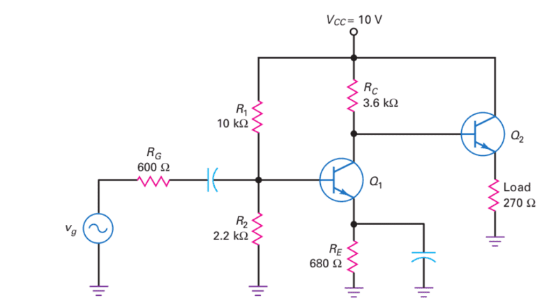
In summary, the CE-CC cascade amplifier discussed in the conversation has a direct connection between the emitter output of Q1 and the input of Q2, without any coupling capacitor or voltage divider bias. This can potentially damage Q2's base-emitter junction if there is an unwanted output voltage from Q1's collector. The calculations for input impedance would change in this case, taking into account the internal emitter resistance of Q2 and the base biasing resistors. To maintain an AC gain of -50, the output impedance, impedance matching, and bias resistor values must be considered. The conversation also suggests simplifying the circuit and calculating one stage at a time. Transistors with high hFE are assumed, allowing for the neglect of loading
  • #1
PhysicsTruth
117
18
Homework Statement
Given a CE amplifier with gain of about -50, design a buffer emitter follower, mentioning all the parameters that can be controlled by the designer, and connecting the load resistance such that the voltage gain isn't affected.
Relevant Equations
##Z_{in} = \beta (r_{e}+R_{C})##
##A_{v} = -(R_{C}||Z_{in})/r_{e}##
Here is a common CE-CC cascade amplifier-
end10.png


Here, the output of the emitter amplifier is directly connected to Q2, without any coupling capacitor or any voltage divider bias. This may harm the base-emitter junction of Q2 in case of unwanted output voltage from Q1 collector. But in that case, the calculations would change completely, where ##Z_{in}## would be perhaps ##RB1||RB2||[\beta(r_{e} + R_{C})]##, where r_e would be the internal emitter resistance for Q2 and RB1,RB2 are the base biasing resistors. How to account for the output impedance, the impedance matching and the bias resistor values in this case, such that the AC gain remains at -50?
 
Physics news on Phys.org
  • #2
Since transistor types and gains are not given, you can assume transistors with very high (almost infinite) hFE. This allows you to ignore loading effects between succesive stages.

From there you might try simplifying the circuit and calculate one stage at a time. For instance, assume that Q2 does not exist and find the DC operating point of Q1, etc.

Since signal frequency and capacitor values are not specified, they can be 'assumed to be appropriate' for the circuit.
 

1. What is a CE-CC cascade amplifier and why is an alternative design needed?

A CE-CC cascade amplifier is a type of electronic amplifier circuit that uses two stages, a common-emitter stage and a common-collector stage, to provide high gain and low output impedance. An alternative design may be needed to improve certain performance characteristics, such as bandwidth or linearity, or to reduce cost.

2. What are some common alternative designs for a CE-CC cascade amplifier?

Some common alternative designs for a CE-CC cascade amplifier include using different types of transistors, such as field-effect transistors (FETs) or bipolar junction transistors (BJTs), or using different biasing configurations, such as self-bias or fixed bias.

3. How do these alternative designs impact the performance of the amplifier?

The impact of alternative designs on the performance of the amplifier can vary depending on the specific design chosen. Some designs may improve certain characteristics, such as bandwidth or linearity, while others may have trade-offs, such as increased cost or complexity.

4. Are there any limitations to using alternative designs for a CE-CC cascade amplifier?

Yes, there can be limitations to using alternative designs for a CE-CC cascade amplifier. Some designs may not be compatible with certain types of input or output signals, or they may require additional components or adjustments to achieve optimal performance.

5. What are some factors to consider when choosing an alternative design for a CE-CC cascade amplifier?

When choosing an alternative design for a CE-CC cascade amplifier, some important factors to consider include the desired performance characteristics, cost, availability of components, and compatibility with other components in the circuit. It is also important to carefully evaluate and test the chosen design to ensure it meets the desired specifications.

Similar threads

  • Engineering and Comp Sci Homework Help
Replies
4
Views
2K
  • Engineering and Comp Sci Homework Help
Replies
7
Views
898
  • Engineering and Comp Sci Homework Help
Replies
17
Views
2K
  • Engineering and Comp Sci Homework Help
Replies
3
Views
1K
  • Engineering and Comp Sci Homework Help
Replies
8
Views
1K
  • Engineering and Comp Sci Homework Help
Replies
23
Views
3K
  • Engineering and Comp Sci Homework Help
Replies
24
Views
2K
  • Engineering and Comp Sci Homework Help
Replies
7
Views
2K
  • Engineering and Comp Sci Homework Help
Replies
25
Views
8K
  • Engineering and Comp Sci Homework Help
Replies
8
Views
2K
Back
Top