High-Power Switching using MOSFETs

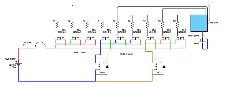
In summary, the circuit includes three MOSFETs wired inline in order to electronically switch a high-current circuit between two inductors. The purpose is to switch one inductor off in order to cool it before starting again. The current delivered to each inductor should be around 75A at 12VDC.
  • #1
nuggetchris
5
0
For a project, I need a means of switching a high-current circuit between two inductors. The purpose is, each inductor serves as an electromagnet, and they are switched every 15s or so in order for one of the two to cool before starting again. The system I've designed uses arduino as a controller and a couple of MOSFETs wired inline in order to electronically switch the circuit. The current delivered to each inductor should be around 75A at 12VDC. In this specific example, I used three 35A rated MOSFETS in each 'bank' which would function similar to a single relay. Here is the schematic:
Revised-1-4.png


Bank B of MOSFETs is a splice from green line to Bank C. The idea is that Bank A will act as a supply switch (Open = NO Power), Bank B (Closed = IND1 ON, IND2 OFF), Bank C (Closed = IND1 OFF, IND2 ON). **The supply switch acts to isolate IND2 from IND1** . To the contrary, with not having the supply switch and splice, the only way I could supply power to the second inductor is if I were also supplying it to the first. That is why I have included the leftmost *third* bank instead of a simple 2, since I need to bypass power past the first inductor.

I am asking for a few aspects:

1) I feel I need more diodes in the circuit to protect against kickback. Have the diodes been added in the right places?

2) Are all the connections correct for the switches and the circuit to function? (Specifically the MOSFET banks and Source/Drain)

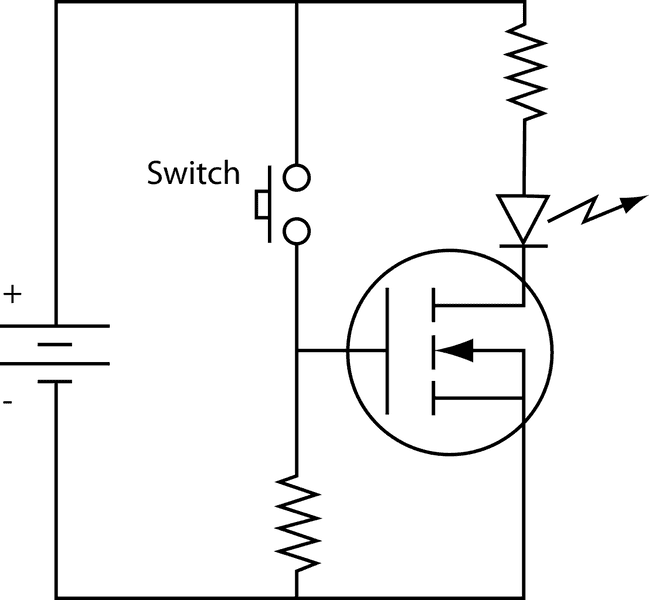
Here is an image I've found of an example NCH circuit:
UDLN3.png


It would appear from this image, that I *do* in fact have the connections of source and drain for each MOSFET wired correctly, with source on the positive end and drain on negative end. Please clarify if it is wrong.

3) Is there a solution to the issue of MOSFETs not turning on at the same VGS, leading to overload/explosion?
 

Attachments

  • g3r9a.png
    g3r9a.png
    11.4 KB · Views: 449
  • UDLN3.png
    UDLN3.png
    7.9 KB · Views: 793
  • Revised-1-4.png
    Revised-1-4.png
    12.1 KB · Views: 1,216
Engineering news on Phys.org
  • #2
First thing is the schematic you have posted has the fet drain to bat positive, and source to the load, this is fine functionally as long as your gate drive is able to float, when "ON" the source will be ~ same voltage as drain, and therefore the voltage to the gates has to be +ve voltage supply + 12V.

Typically with low side drive, which is much easier, the FET source should be to negative, and the load between +ve and fet drain, although depending on the application this may not be permissible for safety/corrosion reasons.

Then if you are using mosfets "rated" at 35A to push 35A, then the case had better be 25C or lower. The better way to do it is look at on resistance, work out your losses and combine that with your heatsink performance to make sure your die are within temp spec.

To work out the diode rating, calculate how much energy stored in the inductor and then work out if the diode can handle the pulse due to discharging it.
 
  • #3
essenmein said:
First thing is the schematic you have posted has the fet drain to bat positive, and source to the load, this is fine functionally as long as your gate drive is able to float, when "ON" the source will be ~ same voltage as drain, and therefore the voltage to the gates has to be +ve voltage supply + 12V.

Typically with low side drive, which is much easier, the FET source should be to negative, and the load between +ve and fet drain, although depending on the application this may not be permissible for safety/corrosion reasons.

Then if you are using mosfets "rated" at 35A to push 35A, then the case had better be 25C or lower. The better way to do it is look at on resistance, work out your losses and combine that with your heatsink performance to make sure your die are within temp spec.

To work out the diode rating, calculate how much energy stored in the inductor and then work out if the diode can handle the pulse due to discharging it.

Hi, the mosfets would not be all pumping 35A, the current I would flow through would only be around 75A, so between three 35A rated fets, that leaves 30A worth of buffer or ~10A buffer on each. I’m located in central Florida in the summer so it may reach ambient temps of ~85F. Accounting for heat generation inside the case I could estimate operation temps of around 100F. However this is all estimation.

How big of a pulse do these diodes normally encounter?

Lastly, I understand your reasoning for moving inductors above drain. I will consider it strongly. What kind of safety issues may arise, and what makes it easier than the current method?
 
  • #4
The problem with current ratings on mosfets is that its essentially calculated from the thermal resistance of the part, its a number that says "this is how much DC current this device will take if you have an infinite heatsink on the case maintained at 25C and you let the junction temperature reach maximum (usually 175C, don't know what this "F" is...).

This is usually a hilariously large number compared to how you can actually run the device once you factor in all the real thermal resistances to ambient.

For your current circuit, you need a gate driver that can have its reference move from ground to positive, since it must be referenced to the FET source, the benefit of your circuit is that when the FETs are "OFF" the inductor coils are connected to negative. So if they are exposed to the outside, they are less likely to suffer from electrically aided corrosion since they have the same potential as everything else.

The low side drive circuit is much simpler, you can take the output of your micro and with some level shifting drive the fet gate, however your coils will be at 12V potential when "OFF", in which case it will help galvanic corrosion and if you have an accident and experience a puncture failure, where the thing is stabbed by other metal, will cause a chassis to battery short = fire.

Neither is wrong, just different pros and cons.
 
  • #5
I am not planning on any puncture failures, as everything is clamped down very securely in the case. My main concern is magic smoke from faulty circuitry. Assuming that, the low side drive circuit would NOT require a gate driver and I can switch using Arduino?

And in order to manage heat, I will go into a bit more detail. The device measures 4ft by 1ft, and each inductor is a large 6.5 inch diameter by 6 inch cylinder, both occupying about 2.5-3ft in the case when installed. On the upper wall of the case behind each inductor is a fan, 2 in total, to cool the inductors and the interior. I am not planning on adding complex liquid cooling, or refrigeration systems. Assuming I depend on these case fans to keep it thermally stable inside (say, 38C average) , what would be the best way to manage the amount of heat generated - opt for higher rated mosfets, heatsink the exteriors of the inductors to kingdom come, what would you do?
 
  • #6
Your FETs aren't going to produce significant heat (< 5W, unless you choose poorly, or under-drive them) - You'll want a heat sink for them, but removing that heat won't be too tough (compared to your other problem): The magnet power will be about 900 W. I'm not sure how much good heat-sinks on the magnets are going to do - the big problem will be getting the heat out of the internal windings (you can probably keep the outside windings cool with air flow). Assuming that this is commercial magnet, the manufacturer should have a datasheet which describes cooling requirements. If it's 'roll your own,' You may need to instrument one and see how much power you can tolerate. They are going to heat a lot faster than they cool.
 
  • #7
Dullard said:
the big problem will be getting the heat out of the internal windings (you can probably keep the outside windings cool with air flow).
There is only one layer of windings, no overlap of coil wire. I'll heat sink the fets, run the fans constantly, and see long I can run each magnet before heat gets excessive. Then refine from there on.
 
  • #8
A single layer is great! You might just make that work - you'll need some serious exhaust fans and some shrouds/ducting. Good luck!
 
  • #9
You really will need a gate driver. The dissipation on switching elements depends on the switching time, and with just the controller, it won't be low enough.

Also, for stopping DC 75A on an inductive load - in this configuration the diodes will take on all the energy what remained in the coils. I don't know how big is the inductance there, but you better pick some big fat * diode, or add some RC elements to share the load.
 
  • #10
I've since updated the schematic a good bit, and it now looks like this:

https://forum.allaboutcircuits.com/attachments/fet-switch-jpg.157706/

Where should diodes go? Across each load? Across each mosfet?
 
  • #11
Not sure if its just me, but can't see the image...
 
  • Like
Likes Tom.G
  • #12
nuggetchris said:
Assuming that, the low side drive circuit would NOT require a gate driver and I can switch using Arduino?
The trick to switching high currents is to switch quickly. That will require a momentary gate drive of about 500mA per MOSFET to charge the gate capacitance. Ideally you need either zero voltage or zero current as heat is W = V * I. The parameter to minimise is decided by duty cycle and frequency.
For high duty cycle, select a low on-resistance device, W = I2 * R.
For high frequency switching, select a low gate capacitance device. Remember that both turning on and turning off should be fast.

It is unnecessary to use an extra bank of MOSFETs as the main power switch. If you place two AND gates in the logic level signals it will halve the W = I2 * R losses and cost less for components and mounting hardware. You need a MOSFET driver to deliver the gate charge current. That can probably be enabled to operate as a master power switch. A driver chip will cost less than a MOSFET.

N-channel MOSFETs cost less, are faster, and have lower Ron, than do P-channel. N-channel work well as low side-switches with logic level drive. If you must use a high-side switch it should be an N-chan MOSFET or IGBT, and you should use a gate driver IC that will perform the logic level conversion and provide the floating supply and gate drive.

A MOSFET that incorporates a schottky diode makes a good flyback diode because you can make it a very efficient diode by short circuiting the diode with the MOSFET during off times. Your circuit could be built from a couple of half-bridge drivers driven by the Arduino. If you select the right components it may not require a heatsink.

I look forward to seeing your latest schematic when it appears.
 
Last edited:
  • Like
Likes Klystron
  • #13
Keep in mind the OP is using this more like a relay than PWM.

"they are switched every 15s or so in order for one of the two to cool before starting again"

I think its fairly safe to say you can ignore switching loss, main thing is enough voltage on teh gate so rdson is minimized.
 
  • Like
Likes Averagesupernova
  • #14
essenmein said:
I think its fairly safe to say you can ignore switching loss...
Depends on the type of the FET. If it is something old-style with lots of copper, then you are right. If it is something new, like a ThinPak or so, then (without carefully designed cooling) even one slow switching might give it enough Joules to cook it.

Sometimes closely available heat capacity is a must.
 
  • Like
Likes Klystron
  • #15

1. What is a MOSFET?

A MOSFET (Metal-Oxide-Semiconductor Field-Effect Transistor) is a type of transistor that is commonly used in electronic devices for switching and amplification. It consists of three terminals - source, drain, and gate - and can be either an N-channel or P-channel device.

2. How does a MOSFET work?

A MOSFET works by controlling the flow of current between its source and drain terminals using a voltage applied to its gate terminal. When a positive voltage is applied to the gate, it creates an electric field that allows current to flow between the source and drain. When a negative voltage is applied, it blocks the flow of current.

3. What is high-power switching?

High-power switching refers to the process of controlling the flow of high levels of electrical power using electronic switches. This is typically done to turn on or off large electrical loads, such as motors or lights, in a controlled and efficient manner.

4. Why are MOSFETs commonly used for high-power switching?

MOSFETs are commonly used for high-power switching because they have a low on-resistance, meaning that they can handle high levels of current without overheating. They also have a fast switching speed, making them ideal for applications that require quick response times.

5. How do you design a circuit for high-power switching using MOSFETs?

To design a circuit for high-power switching using MOSFETs, you need to consider factors such as the maximum voltage and current ratings of the MOSFET, the load characteristics, and the required switching speed. You will also need to properly size and connect external components, such as gate resistors and flyback diodes, to ensure the safe and efficient operation of the circuit.

Similar threads

  • Electrical Engineering
Replies
12
Views
1K
Replies
42
Views
2K
  • Electrical Engineering
Replies
1
Views
909
  • Electrical Engineering
Replies
1
Views
826
Replies
39
Views
3K
  • Electrical Engineering
Replies
12
Views
1K
Replies
7
Views
2K
  • Electrical Engineering
Replies
28
Views
3K
Replies
18
Views
5K
Replies
37
Views
3K
Back
Top