I don't understand transistors in combinations .... Or maybe basics ....

In summary,The transistor can solve problems by providing a voltage and current at the base and collector. The transistor is controlled by the resistors in the circuit.
  • #1
Xenon02
62
6
Hello everybody !
I do have a problem understanding transistor.
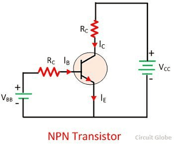
I know how these solve and work :
1664566409226.png

I know some basics like the voltage on Rb is Vbb - 0,7V. Or something like this.
I also Know that the maximal current in this transistor is "defined" by the resistor in the collector which is RC. So Vcc/Rc = Ic_max.
Those are my basics I understand so far, so increasing current Ib increases the current Ic and the voltage Vce is dropping to the point where is it equal 0,2V or 0,1V (saturation).
So everything is defined here by resistors. Okey I understand it.
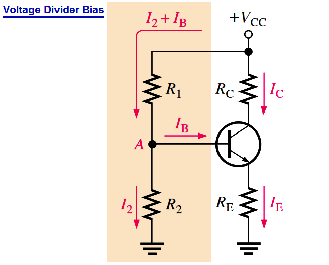
But then I tried to understand more "complex" circuits for example this one :
1664566891415.png

So I thought that : if it wasn't voltage divider but normal voltage source then Vb is equal the voltage source for example it is 5V so the voltage on RE should be 5V - 0,7V = 4,3V I get it. But then I tried with voltage divider let's say R1 and R2 are equal (10k) and the Vcc = 10V so the voltage on R2 should be 5V right ? So Vb = 5V. But when I connected the transistor then Vb changes to different value changes in the R2 ... Dunno why I used the basic principles of the transistor. I've heard that it acts like a load or a diode but I don't get it ...
Then I've heard that Ve can change as well as Vb ... so changing the value of resistor not only changes the Ve but also the Vb ...

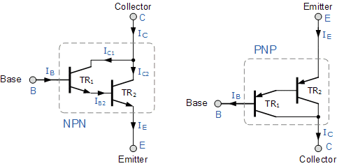
Or here :
1664567014426.png

How is it possible that connecting transistors with each other works ?
How is the current even defined there ? I know from the first picture (basics) that voltage and current in transistors are defined by the resistors. Okey you can say that I can connect resistors in the C or E or B point like in the picture, but the emiter of Tr1 doesn't have a typical connection like in the basics. Basics covered that resistors defined everything now I have in the emiter of Tr1 the base of Tr2. How does it work ? When I will reach the max current value ? How does the voltage change in Vce_1 or Vce_2 if there is this uncommon for me connection in emiter of Tr1 connected to base of Tr2.

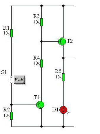
I also tried this one as well :
1664567211999.png


It's so hard ...
Because when I change the value of voltage or resistor, makes me think how to create my own circuit with transistor that can work in active region or saturation if I had AC power supply or potentiometer in one of these resistors. Checking every Vb_1.Vb_2 ,Vb_3 etc or Ve_1 Ve_2 Ve_3. The current every where and my god there is so much details ...
Sorry if this place is not for my "basics" problem with transistors. But I don't understand how to anylize circuits in transistor not looking at every details ... there is so many things to look at ...

Also a small note : I'm a bit stubborn with some stuff that I've learned from basics or from somewhere if I will repeat myself not understanding something the same thing, I'm sorry.
 
Engineering news on Phys.org
  • #2
R1 and R2 must not be too high in value; they should swamp out the current drawn by the transistor base.
 
  • #3
tech99 said:
R1 and R2 must not be too high in value; they should swamp out the current drawn by the transistor base.
I mean cool :D
But I don't understand how basics work in more "complex" circuits that I've written all about :D
 
  • #4
The basics are about current, don't be distracted by voltage.

For a big current to flow in the collector-emitter circuit, a small current must flow in the base-emitter circuit. The circuit surrounding a BJT, allows those currents to flow in a controlled and useful manner.
 
  • Like
Likes DaveE
  • #5
Baluncore said:
The basics are about current, don't be distracted by voltage.

For a big current to flow in the collector-emitter circuit, a small current must flow in the base-emitter circuit. The circuit surrounding a BJT, allows those currents to flow in a controlled and useful manner.
But with current comes voltage.
I mean if there is Vbe < 0,7V then even the current won't do the job.
So checking voltage is also a part I guess ?
Also something must controll/limit the current. But transistor itself cannot controll/limit how much current he receives to base "Ib" (resistors usually limits the current) so connecting 2 BJT like in darlington somehow works, even though they cannot controll/limit the current. I mean that base of the Tr2 receives the current from Tr1, so when do I know that Tr1 reached the maximum current collector value, when on the emiter is base of Tr2. But this base doesn't have any limits.
Or in voltage divider. The transistor doesn't have Rb in the base that will limit the current but it works that's one thing and another one is that the voltage on R2 (second picture) drops drastically, even if the voltage on him was Vcc/2.
It's hard to see how it works and why it works. I know that there must be something that limits the current.
 
  • #6
I suggest getting rid of the transistor and substituting a simpler model for it. Once you are comfortable with that, you can use more complicated models. Always start with the simplest ("T") model for DC/Bias questions. Then, for AC analysis, remove the diode and add in the emitter resistance, add capacitors for bandwidth/stability questions. Models can get extremely complex, but the truth is those are seldom used by most EEs.
https://electronics-course.com/bipolar-junction-transistor-bjt
 
  • Like
Likes Xenon02
  • #7
Xenon02 said:
But with current comes voltage.
Currents usually require external voltages, but understanding BJT currents is more fundamental. The internal currents must be understood first, independent of the external circuit. For silicon, VBE ≈ 0.7 V is a distracting secondary detail. For most circuit understanding, you can assume VBE is near zero.

Stop arguing, you will be lost until you think about the care and feeding of current to the BJT first.
 
  • #8
DaveE said:
I suggest getting rid of the transistor and substituting a simpler model for it. Once you are comfortable with that, you can use more complicated models. Always start with the simplest ("T") model for DC/Bias questions, then add in the emitter resistance for AC analysis. Models can get extremely complex, but the truth is those are seldom used by most EEs.
https://electronics-course.com/bipolar-junction-transistor-bjt
I've seen somewhere this link, it was also interesting.
I've also mentioned that I've tried to understand transistors from the very basics :D
Using just simple one transistor and having fun with him in the simulator. I know that Vbe is something like a diode. But something must limit the current that goes throught base as far as I know.
That's why I was confused seeing darlington transistor.
Maybe what I've written in the 1# Post might be wrong but the basics kinda makes me more confused. Adding more resistors etc. or even adding another transistor.
Because I don't know what to focus on :D The current, the Voltage on the Base or the Voltage on the Collector or other stuff.
the stuff that Vb changes and Ve also changes. Like nothing is constant. It's hard to for me to find a rule that can let me operate with transistors.
I might sound pretty stupid but maybe I'm weird that transistors are a bit weird itself. I've tried to make a circuit with LED that works when there it's dark and it doesn't work when it's bright outside. But it was hard for me to "calculate" when the Vb changes constantly as well as Ve (of course Vbe doesn't change).
 
  • #9
Xenon02 said:
But something must limit the current that goes throught base as far as I know.
The emitter voltage will rise due to emitter current in the emitter circuit impedance, until the base current is limited, which will feedback to limit the emitter current.
 
  • #10
Baluncore said:
The emitter voltage will rise due to emitter current in the emitter circuit impedance, until the base current is limited, which will feedback to limit the emitter current.

Sorry I don't understand it ?
Okey maybe something like this :

1664584652143.png

Here I can say that the voltage on the Rb is Vbb - 0,7V. So that Vb = 0,7V and Ve = 0V. Okey. Increasing the voltage won't increase the Vb nor Ve instead it will increase the current Ib. increasing Ib increases Ic. Increasing Ic will increase the voltage drop on Rc thus it will decrease the Vc. If we increase enough then the voltage will drop to Vce = 0,2 V which means it is in saturation.
Okey so there is something that limits it and has a direct impact on the single transistor.

Here :

1664584797585.png

I have Re and voltage divider, there is no Rb like before.
Instead of that the current goes directly to this transistor without any limits like before.
So what happens here ? Why does the Vb changes whenever I change a voltage or a resistor ?
How to predict the changes or how to predict in which state it is right now ? is it on active, saturation or cutoff ?

Or here :

1664584935681.png


Here is even worse for me to understand.
From the 1st picture I know that the current has some limits but here ? Base of Tr2 connected to emiter ot Tr1. First and second transistor doesn't have anything that limits the current. But okej let's say we add Rb to Tr1, but still Tr2 doesn't have any limits (there is no Rb2).
I want to know why the second and third picture with transistor works. Because from the basics I don't really know.
 
  • #11
@Baluncore
I'm sorry if I'm repeating something, I just can't imagine how it works basing on the 1st picture that I refere to as a basics. So I tried to do an analize for the first picture and emphezise the problem I have with the other pictures.
I've also noticed that my previous post was pretty rude so I apologize for that.
 
  • #12
Baluncore said:
The emitter voltage will rise due to emitter current in the emitter circuit impedance, until the base current is limited, which will feedback to limit the emitter current.
You were analysing an emitter follower at the time of the quote, not a voltage divider biased voltage amplifier.

Analyse the emitter follower with an emitter resistor only.
Sweep the base voltage from zero to Vcollector.
Then do the same for a Darlington pair.
 
  • #13
Baluncore said:
Analyse the emitter follower with an emitter resistor only.
Sweep the base voltage from zero to Vcollector.
Then do the same for a Darlington pair.

You mean emitter followe like this ?
1664586541834.png

This one was quite interesting to analize.
Because before here :

1664586572095.png


The Vb was constant which was 0,7V.
Now in the first picture Vb can be anything just like Ve can be anything.
So hmmm how it works. Increasing Voltage in base will increase Vb ? Or maybe not ? Because the Ve also changes, the most important part is that Vbe is there.

Looking at this for example :
2022-10-01.png

Well The Vb will be constant which can have any value but Ve will be equal Ve = Vb - 0,7V. So if Vb was equal 5V then Ve equals 4,3V. But adding Rb makes it different ? Increasing Vin when there is Rb doesn't tell me a lot about what will be the Vb. Will it increase or not ?
Also you have mentioned to do the same with Darlington. But how exactly ? Here there are resistors that defines most of the part, in darlington the connection emiter T1 - Base T2 the current is mostly unknown.
Maybe I'm wrong I don't know.
 
  • #14
Xenon02 said:
So hmmm how it works. Increasing Voltage in base will increase Vb ? Or maybe not ? Because the Ve also changes, the most important part is that Vbe is there.
The only important thing is the current gain, beta, β, of the BJT.
 
  • Like
Likes DaveE
  • #15
@Xenon02 it is somewhat clear to me that you are missing some of the basics. The transistor with the voltage divider connected to the base is a LOADED voltage divider. You should realize what happens when you load a voltage divider.
 
  • #16
Xenon02 said:
Also you have mentioned to do the same with Darlington. But how exactly ? Here there are resistors that defines most of the part, in darlington the connection emiter T1 - Base T2 the current is mostly unknown.
A BJT is a current operated device, with a current gain ratio.
You must become the BJT; and then think about currents.

You have been brought to your knees by your fascination and worship of silicon and 0.7 volts. VBE is not 0.7 V.
VBE is proportional to Log( emitter current ).

First, understand the currents in the BJT.
The resistors will be part of the external circuit.
 
  • Like
Likes cabraham
  • #17
Have you worked with simple passive networks yet (Kirchhoff's Laws, etc.)? Your first post says you can understand and solve the first schematic, a simple common emitter circuit, but you have trouble when a couple more resistors are added. That sounds like a circuit problem to me, not a transistor operation problem. The transistor behaves the same way in both circuits, just the applied voltages and currents are different.

Khan Academy has some really good free tutorials on electronics. Check them out.
 
  • #18
Hi @Xenon02

Lets see if this approach helps any.
Refering to the first circuit in post #1 https://www.physicsforums.com/posts/6806170/

(I can't get the circuit to copy here. :cry:)

For a switching circuit an easy way to approach it is this:

1) decide on the Collector current you need
2) divide the Collector current by the transistor Curent Gain (β or Beta)
(this gives you the minimum Base current needed to switch the desired Collector current)​
3) Knowing the needed Base current, you can now select a Base bias voltage and a Base bias equivalent series resistance.

The Base bias voltage selection can be a bit tricky. If this is just for a simulation, you can use the nominal 0.7V for low currents and increase (or decrease!) it in the simulation as needed.

If you want to get detailed or for higher currents, get the transistor datasheet. Look for a graph showing B-E (Base-Emitter) voltage vs Base Current. That is needed because in addition to the nominal 0.7V threshold of the transistor, there is also an internal resistance involved. Knowing your needed Base current, read off the corresponding Base voltage from the graph.

Hope this helps!

Cheers,
Tom
 
  • #19
Baluncore said:
A BJT is a current operated device, with a current gain ratio.
You must become the BJT; and then think about currents.

You have been brought to your knees by your fascination and worship of silicon and 0.7 volts. VBE is not 0.7 V.
VBE is proportional to Log( emitter current ).

First, understand the currents in the BJT.
The resistors will be part of the external circuit.
To Xenon02:
I know that I will meet with opposition here with the following statement. Nevertheless:
The bipolar transistor is undoubtly a voltage controlled element.
(So your sentence in post#5 "I mean if there is Vbe < 0,7V then even the current won't do the job." is pretty close to the truth).
Up to now it was only claimed that it is current controlled - without any proof!
And such a proof is not possible.
But for the fact of voltage control Ic=f(Vbe) there are many proofs, observations and explanations.
(By the way - this view is also confirmed by leading universities, scientists and developers.)
So the stabilization of the operating point with an emitter resistor works only because of the voltage control.
If there is interest, I can list some more here.
But in general: It is physically impossible, that a small base current can control a larger current by the factor 100..200.
 
Last edited:
  • #20
LvW said:
But in general: It is physically impossible, that a small base current can control a larger current by the factor 100..200.
Please explain or provide a link.
 
  • #21
Sorry - my sentence was not complete:
But in general: It is physically impossible, that a small base current can directly control a larger current by the factor 100..200. (This should be clear simply from the energy point of view).
But it would be interestig for me to see some (at least one) verification for current control of the BJT.
 
  • #22
LvW said:
Sorry - my sentence was not complete:
But in general: It is physically impossible, that a small base current can directly control a larger current by the factor 100..200. (This should be clear simply from the energy point of view)
That depends on what you mean by directly.

From the energy point of view, current is not energy.
 
  • #23
Baluncore said:
From the energy point of view, current is not energy.
Electrical energy itself can be expressed as the electrical power multiplied by time:
E=P*t=E=I²R*t
 
  • #24
Okey I see that we are we moving away from the topic :D

Okey let's start with this :
Baluncore said:
A BJT is a current operated device, with a current gain ratio.
You must become the BJT; and then think about currents.

You have been brought to your knees by your fascination and worship of silicon and 0.7 volts. VBE is not 0.7 V.
VBE is proportional to Log( emitter current ).

First, understand the currents in the BJT.
The resistors will be part of the external circuit.

Basically Transistor is about current which I understand because in active Ic = Ib*B (I don't know how to make beta to it will be a big B :D)
But usually how do I know what is the current that is provided to the base ? or to the collector ?
I have to use resistors.
But how to understand the current in more complex transistors ? Like in the divider (or a divider with potentiometer) ? There are so many factors to look at or when the Vbe isn't sufficient or that Vce is saturated.
Averagesupernova said:
@Xenon02 it is somewhat clear to me that you are missing some of the basics. The transistor with the voltage divider connected to the base is a LOADED voltage divider. You should realize what happens when you load a voltage divider.

I also thought of that the base is some form of load.
But I was just referring to that Vbe is equal 0,7V or less it doesn't matter. The thing is that if voltage divider had 5V then using this simple Vbe I could predict the rest. I could also predict the current and everything.
Using a potentiometer in on of the resistors causes me a lot of problem because I don't know when the transistor is active/saturated/cutoff.
Even better what if I use voltage divider in a collector of a transistor and connect another transistor like here :
1664622603093.png

Now hehe, I tried to understand why it works this way, why is it saturated etc, or why isn't it active or cutoff.
DaveE said:
Have you worked with simple passive networks yet (Kirchhoff's Laws, etc.)? Your first post says you can understand and solve the first schematic, a simple common emitter circuit, but you have trouble when a couple more resistors are added. That sounds like a circuit problem to me, not a transistor operation problem. The transistor behaves the same way in both circuits, just the applied voltages and currents are different.

Khan Academy has some really good free tutorials on electronics. Check them out.
I do know Kirchoff's Laws, Norton/Thevenin equivelants, Ohm Laws.
It's just that transistor behavies differently and wierdly for me. I can't predict anything what happens here :D

LvW said:
To Xenon02:
I know that I will meet with opposition here with the following statement. Nevertheless:
The bipolar transistor is undoubtly a voltage controlled element.
(So your sentence in post#5 "I mean if there is Vbe < 0,7V then even the current won't do the job." is pretty close to the truth).
Up to now it was only claimed that it is current controlled - without any proof!
And such a proof is not possible.
But for the fact of voltage control Ic=f(Vbe) there are many proofs, observations and explanations.
(By the way - this view is also confirmed by leading universities, scientists and developers.)
So the stabilization of the operating point with an emitter resistor works only because of the voltage control.
If there is interest, I can list some more here.
But in general: It is physically impossible, that a small base current can control a larger current by the factor 100..200.
Voltage is also involved as I can understand ?
That's why many things are mixing up in my head ...

So yea from the quotes I have used here maybe you can understand why I am confused ?
I just know how the circuit from the Post#1 works as I have analized it. But with other circuits I have problem. Like how to approach them, or why it works this way.
For example how to approach normally transistors. Or how should I understand the connection like in Darlington ? Or like in the divider or like divider + another transistor.
What is limiting the current for those transistors ? If not the resistors like in 1st picture in Post#1 then what is ?

Ayayay :D
When I look at the picture I am sending in this post I just get confused :D So many factor to look at, voltage on T2 current in T2 what is limiting the IB (because there is no Rb).
In other words my mindset is stuck in the first circuit from the picture in Post#1. That Rb controlls the current but in other circuits it is different. I can't understand them from the pictures of transistors tutorials.
 
  • #25
Quote Xenon:
Voltage is also involved as I can understand ?
That's why many things are mixing up in my head ...
......
So yea from the quotes I have used here maybe you can understand why I am confused ?
I can't understand them from the pictures of transistors tutorials.

___________________________________________________________________________________________________________________
Xenon 02, I can fully understand that you feel confused.
Let me explain:
1.) It can be shown, prooved and verified that the emitter- and (with it) the collector current is controlled solely by the voltage Vbe. This is according to the well-known Shockley equation Ie=f(Vbe) with Ie=Ib+Ic.
The base current is nothing else than a very small part of Ic (and must be seen as a kind of non-ideality or an unwanted side effect).

2.) The well-known equation Ib=Ic/B is, of course, correct but if used in the form Ic=B*Ib it must not be interpreted as a relation between cause and effect.

3.) The problem now is two-fold:
(a) In some books and other contributions (papers and internet forums) the BJT unfortunately is described as current controlled (just a claim without any verification).
This is really a phenomenon - and it is simply false. This results from a false interpretation of the relation Ic=B*Ib.

(b) There are two mostly used small-signal equivalent diagrams for the BJT and one of the two contains the current-controlled view using a current source controlled by B (resp. beta). For some calculations, this works of course and can be used (because the formula Ic=B*Ib is correct) - however, this diagram must not be used as a basis for explaining how the BJT physically works.
In contrast, the other small-signal representation with a transconductance gm in the output circuitry mimics the physical truth.
Remember: Transconductance gm is the slope of the Ic=f(Vbe) characteristic gm=d(Ic)/d(Vbe). This results in gm=Ic/Vt and - surprisingly - for gain calculations, also the current-control defenders are using this expression (which results from the voltage-control function!)

4.) Resume: For some calculations you can use the current-controlled view (sometimes simpler) - however, if you want to understand the working principle of transistor-based circuits you will have no success with current-control (Why emitter resistor? Why low-resistive base divider? How works the current mirror? What is the Early effect? What means the tempco of -2mV/K ? Why Vbe<0.6V for class B-operation?...).
There are many effects and observations (and circuit principles) that can be only explained with the voltage-control view.
 
Last edited:
  • #26
Xenon02 said:
Basically Transistor is about current which I understand because in active Ic = Ib*B (I don't know how to make beta to it will be a big B :D)
But usually how do I know what is the current that is provided to the base ? or to the collector ?
I have to use resistors.
β is available from the symbol menu in the toolbar, maybe you need to press [ ] first to toggle BB mode.

You know that the connection between the input circuit and output circuit will be through the transistor, and that the current ratio will be β. Assume zero base current, then guess at the base bias voltage. Assume that the emitter voltage is equal to the base voltage. Estimate the emitter current. Use β to compute the required base current. Refine the estimates until you understand the circuit that contains the BJT. There is no one strategy to analysing all BJT circuits.

You include so much in one post that you will confuse yourself and anyone who tries to help you.
 
  • #27
@Xenon02 the schematic in post #24 is a very simple one. Based on what you say you grasp you should be able understand it. Please keep your posts shorter. Starting at the push button switch, what are you having trouble with?
 
  • #28
LvW said:
Xenon 02, I can fully understand that you feel confused.
Glad to hear it :D
LvW said:
1.) It can be shown, prooved and verified that the emitter- and (with it) the collector current is controlled solely by the voltage Vbe. This is according to the well-known Shockley equation Ie=f(Vbe) with Ie=Ib+Ic.
The base current is nothing else than a very small part of Ic (and must be seen as a kind of non-ideality or an unwanted side effect).

2.) The well-known equation Ib=Ic/B is, of course, correct but if used in the form Ic=B*Ib it must not be interpreted as a relation between cause and effect.
If not cause and effect then what ? About point nr.2
LvW said:
3.) The problem now is two-fold:
(a) In some books and other contributions (papers and internet forums) the BJT unfortunately is described as current controlled (just a claim without any verification).
This is really a phenomenon - and it is simply false. This results from a false interpretation of the relation Ic=B*Ib.

(b) There are two mostly used small-signal equivalent diagrams for the BJT and one of the two contains the current-controlled view using a current source controlled by B (resp. beta). For some calculations, this works of course and can be used (because the formula Ic=B*Ib is correct) - however, this diagram must not be used as a basis for explaining how the BJT physically works.
In contrast, the other small-signal representation with a transconductance gm in the output circuitry mimics the physical truth.
Remember: Transconductance gm is the slope of the Ic=f(Vbe) characteristic gm=d(Ic)/d(Vbe). This results in gm=Ic/Vt and - surprisingly - also the current-control defenders are using this expression !

4.) Resume: For some calculations you can use the current-controlled view (sometimes simpler) - however, if you want to understand the working principle of transistor-based circuits you will have no success with current-control (Why emitter resistor? Why low-resistive base divider? How works the current mirror? What is the Early effect? What means the tempco of -2mV/K ? Why Vbe<0.6V for class B-operation?...).
There are many effects and observations (and circuit principles) that can be only explained with the voltage-control view.

And this is the part where I get confused.
So how should I analize the transistors ?
Basing on the potentials such as Vc,Ve and Vb (potential on collector,emiter,base), on the current Ib, Ic ? Or everything ?
How exactly should I look at transistors for example in Post#1 picture 2 or picture 3.
Here I have made a analize for picture nr 1.
Xenon02 said:
Okey maybe something like this :

1664584652143-png.png

Here I can say that the voltage on the Rb is Vbb - 0,7V. So that Vb = 0,7V and Ve = 0V. Okey. Increasing the voltage won't increase the Vb nor Ve instead it will increase the current Ib. increasing Ib increases Ic. Increasing Ic will increase the voltage drop on Rc thus it will decrease the Vc. If we increase enough then the voltage will drop to Vce = 0,2 V which means it is in saturation.
Okey so there is something that limits it and has a direct impact on the single transistor.

In which I have analized everything. Vc, Vb, Ve, Ib and Ic.
I know why Ib has a specific value as well as Vb and other stuff here.
For emiter resistor it was a bit harder because Vb and Ve changes whenever I change something which is unpredictable for me. Of course I'm not using exact numbers, I'm trying to understand the intuition how enerything works.
I've tried with emiter like here in the Post#13.

But It was harder to understand how it exactly works.
So what should I look at. The current Ib, Ic or the voltage Vb,Vc and Ve ?
What makes the transistor works for Darlington or for divider if there is no Rb that can define the Ib.
Sorry if I'm repeating again something.
Baluncore said:
You include so much in one post that you will confuse yourself and anyone who tries to help you.

I'm sorry, I just don't know how to convey what I have issue with in short ;)

Averagesupernova said:
@Xenon02 the schematic in post #24 is a very simple one. Based on what you say you grasp you should be able understand it. Please keep your posts shorter. Starting at the push button switch, what are you having trouble with?

Well in the schematic from post#24 the problem basically is that there are 2 transistor connected to each other + there is a voltage divider. I only know what I analized in Post#10 and Post#13 but with 13 it was a bit problematic.
first of all I don't know what is the current or rather what is limiting the current that flows from PNP which is T2, There is no Rb like in the Post#1 picture 1. Also this is voltage divider so calculating the Vb and Ve (here is actually 0V for Ve). But still the voltage divider + transitor just changes the Vb so if I calculated the voltage divider that has a specific value and it changes then the whole circuit behavior also changes.
Basically I don't get it why everything here works and how do they work (active,saturation,cutoff which one and why?) Or if I had a potentiometer or AC supply I cannot predict what is going to happen. For the post#1 picture 1 I could predict it even if I had potentiometer or AC supply connected to it because everything works like in the analizys.
 
  • #29
So do you get confused if you draw in a resistor from base to emitter in the second schematic in post #13? Think carefully here.
 
  • #30
Xenon02 said:
So how should I analize the transistors ?
Basing on the potentials such as Vc,Ve and Vb (potential on collector,emiter,base), on the current Ib, Ic ? Or everything ?
Xenon02 - you are asking so many questions...it is not easy to give a comprehensive answer.
Perhaps the following list of steps may help. Here I have described how I would design a simple gain stage as shown in your 1st post (second circuit, figure 2):Step 1: Based on (a) the available supply voltage Vcc and (b) the required/wanted voltage gain Av you must select a collector resistor Rc and a DC quiescent current Ic. In this context, the following formula is essential
Av= - gmRc (with transconductance gm=Ic/Vt).
(Comment: The transconductance gm desribes the slope of the voltage control function Ic=f(Vbe))

Step2: Use an emitter resistor Re with a value of app. 10% of the Rc value (rule of thumb).
The DC voltage drop on (Rc+Re) should be app. 50% of the available DC supply Vcc.
From this we can derive an expresssion which gives a good „feeling“ for the maximum possible voltage gain (ignoring Re as a first guess):
Av= - gmRc= - (Ic/Vt)(Vcc/2)/Ic= - Vcc/2Vt (with app. 2Vt=50mV)
A gain reduction is always posible using signal feedback (step 5).

Step 3: Using the known DC voltage Ve at the emitter and with Vbe=0.7 V the required base voltage is Vb=Ve+0.7V.
This DC bias voltage should be created with a simple voltage divider (R1, R2) at the base. You are free to select the resistive niveau of this divider chain but there are some constraints (step 4) .

Step 4: The total input resistance should not be too small (with respect to the properties of the driving signal source) - on the other hand, the resistors should allow a DC current through the chain that is remarkably larger than the expected base current Ib=Ic/B (which goes through the upper resistor R1). It is the goal of this „trade-off“ to enable a „stiff“ base voltage Vb (which does not remarkably depend on the very large tolerances of B - another indication for voltage-control).

As a rule of thumb: Current through R1 is app 10*Ib.

Step 5: The emitter resistor Re (or a part of it) can be bypassed with a capacitor Ce. This is because Re does not provide DC feedback only - at the same time it provides also signal feedback which reduces the gain according to the expression:
Av= -gmRc/(1+gmRe).

When such a gain reduction is not desired the influence of Re on signal properties is eliminated with a capacitor Ce.

Final comment: As you can see, there is not only a simple set of formulas which can/must be used for designing such a gain stage. You still have some freedom during this design phase. This is very important because this gives you the chance to adapt the circuit to some application-specific requirements.
____________________________________________

Regarding the equation Ic=B*Ib you were asking "If not cause and effect then what ? "
My answer: There are many equations in physics and electronics which are correct without telling you - at the same time - something about cause and effect.
Simple example:
Mechanical pressure P is force F per area A: P=F/A.
This can also be rewritten as F=P*A.
Is the force F, therefore, the result of the pressure P on the surface A? No, of course not.

The correct "sequence" is as follows:
Ie=f(Vbe).
Ie=consists of two parts: Ie=Ib+Ic.
With Ic=a*Ie (a close to "1") we have the rest: Ib=Ie-Ic=Ic[(1/a) - 1)] and
Ib=Ic/B with B=a/(1-a).
This can be rewritten as
Ic=B*Ib .
 
Last edited:
  • #31
BJT is ultimately charge controlled. The following terminal equations are used to describe bjt:
Ic = beta*Ib
Ic = Ies *exp ((Vbe/Vt) - 1)
Ic = alpha * Ie
A good simulation program or lab tests will affirm that changes in current happen before change in voltage. A p-n junction has some capacitance, as well as inductance. At the frequencies the bjt operates at, capacitance dominates. The *Vbe* cannot change unless *charge* is injected into the b-e junction in the form of base & emitter currents, Ib & Ie. As soon as Ie changes, Ic changes a moment later, then Vbe eventually "catches up".
The easiest way to see this is to observe a simulation of a signal diode, such as a 1N914B, or 1N4148.
A simulation is attached. Notice how current exhibits the stair case function, while voltage gradually rises to reach the new value. The diodes voltage is determined by its current, not vice-versa.
An i-v graph of the 1N914B diode is attached. The Vbe "barrier value" depends on forward current. At 10 uA current, Vbe is just under 0.40 volt at room temp.
The Shockley diode equation simply describes the relation between I & V. It can be written 2 ways:
1) Is = Is * exp ((Vd/Vt) - 1),
2) Vd = Vt * ln ((Id/Is) + 1).
Just as Id = f(Vd), Vd = f(Id).
For further study, please search using these terms:
Diode reverse recovery
Diode forward recovery.
Finally, we can discuss *Early effect.* it is true that collector current is *slightly influenced* by Vce, collector emitter voltage, but this is relatively small. A 20% increase in Ie results in about a 20% increase in Ic.
But a 20% increase in Vce results in an Ic change *much less* than 20%.
To claim that the bjt is slightly "voltage controlled by Early effect" is not wrong. The key word here is "slightly".
 

Attachments

  • i-v diode2 wav.pdf
    30 KB · Views: 78
  • i-v diode2 sch.pdf
    36.5 KB · Views: 81
  • 1n914b i-v zoom.jpg
    1n914b i-v zoom.jpg
    58.5 KB · Views: 78
  • #32
cabraham said:
The Shockley diode equation simply describes the relation between I & V. It can be written 2 ways:
1) Is = Is * exp ((Vd/Vt) - 1),
2) Vd = Vt * ln ((Id/Is) + 1).
Yes , no doubt about it. So what?
Do you mean to say that when you rearrange an equation, cause and effect are also automatically swapped?
 
  • #33
LvW said:
Yes , no doubt about it. So what?
Do you mean to say that when you rearrange an equation, cause and effect are also automatically swapped?
No! I am saying that cause & effect cannot be determined from this equation. I attached simulation showing I-V response to a staircase generator function. The plot waveform gives insight into which quantity changes first, & which responds to said change later.
 
  • #34
cabraham said:
No! I am saying that cause & effect cannot be determined from this equation. I attached simulation showing I-V response to a staircase generator function. The plot waveform gives insight into which quantity changes first, & which responds to said change later.
I totally agree with you because cause& effect must not automatically derived from any equation.
This is the reason why I only have mentioned physical explanations, real observations and corresponding design techniques in my argumentation (see point 4.) in my post #25).
 
  • #35
@LvW & @cabraham I hate to sound like a jerk but I think it's best to take your level of discussion out of this thread. Some guidance on basic circuit analysis is all that is necessary. At this point, whether the chicken or the egg came first just doesn't matter.
 
  • Like
Likes NTL2009, GrahamN-UK, Tom.G and 4 others

Similar threads

Replies
80
Views
3K
Replies
3
Views
2K
Replies
10
Views
1K
  • Electrical Engineering
Replies
5
Views
2K
Replies
5
Views
2K
  • Electrical Engineering
Replies
19
Views
1K
Replies
16
Views
4K
  • Electrical Engineering
Replies
3
Views
796
Replies
4
Views
959
  • Electrical Engineering
Replies
2
Views
986
Back
Top