Measuring current across biased transistor

In summary: The op-amp inputs require no current, they sense voltage.The SD photo-current, i, flows through R.The op-amp maintains an output voltage so that it's + and – inputs are zero.The op-amp output voltage is therefore Vout = i*R.The “Set VDS” is a ground referenced DC supply that sets the SD bias.You do not need to use a resistor as a current divider, you select an appropriate value for R.
  • #1
PhysicsGuy99
9
0
Hello all,

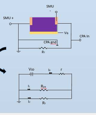
I am interested in measuring the photoresponse of a transistor with a fixed source-drain bias. I would like to feed the drain current into a current preamplifier and output the preamplifier signal to another location. The preamplifier has a very low current maximum, so I will use a current divider. The preamplifier has a known input resistance.

I am using an SMU to provide a constant VSD, and it is important to be able to fix this potential at whatever value I want. I have attached what I can come up with, but I am not sure this is the best approach...

In the cartoon below, I draw a cartoon and a (at least I think so) equivalent circuit. I have modeled the SMU potential across the SD as a battery with resistor in series. The CPA (Current preamplifier) is also modeled as a resistor. I believe the input has to be in series with I1 (current measurement).

I have also included equations for what I think will be I1 and I0.

Any advice for whether this looks reasonable, or improvements would be greatly appreciated!

Thanks.
chd5rmH.jpg
Ms9gVDe.jpg
 
Engineering news on Phys.org
  • #2
It's unclear to me how you are ensuring both a fixed source-drain voltage and using a resistor as a current divider.

It would seem either VSD will change with the current across the resistor, or the current will not be evenly divided if you somehow keep the input to the current amplifier at a constant voltage level.
 
  • #3
What part number is your CPA?
Why did you select it?
What bandwidth do you need for the test?
It is normal to convert the current to a voltage for transmission some distance.
See attached circuit for an example of a junction being operated at a fixed voltage.
i 2V.png
 
  • Like
Likes Jeff Rosenbury and PhysicsGuy99
  • #4
Jeff - The idea was to have the current preamplifier and RT in parallel with the SMU. The SMU is very good at fixing a voltage and supplying whatever current necessary to force that voltage.

Baluncore - The CPA is made by Stanford Model SR570. It can provide a +- 5V bias, so I may just end up using that as the source-drain bias. I selected this because I had no other choice, and I would like to make it work. It is a good piece of equipment, I just need to provide the correct signal input to utilize it properly. Thanks for providing that drawing! That is really helpful. I will have to think about it for a little while to see if it will accomplish what I need.

Currently I am thinking of operating with this set-up:

aODLVC8.jpg


The main issue is that the current preamp can only provide a 5V bias, and I would like to operate an order of magnitude higher.

So from here I will have to see if the circuit Baluncore suggested will work..

Thanks!
 
  • #5
Baluncore said:
What part number is your CPA?
Why did you select it?
What bandwidth do you need for the test?
It is normal to convert the current to a voltage for transmission some distance.
See attached circuit for an example of a junction being operated at a fixed voltage. View attachment 87905

So the way you have VDS set up won't the current just flow from + to - side of the SMU? I don't see why the current would flow through the transistor if it has a direct path from + to -...
 
  • #6
First some clarifications.
1. What does the acronym SMU stand for?
2. The topic title “Measuring current across biased transistor” refers to current. Current flows “through” a device while voltage appears “across” the device. There is a possible misunderstanding of the question.
3. As I understand it, the SD voltage will be fixed while the photo-current flowing will be measured.
4. What will be done with the gate voltage?

My circuit in post #3 is designed so the inverting (–) op-amp input is maintained at zero potential.
The op-amp inputs require no current, they sense voltage.
The SD photo-current, i, flows through R.
The op-amp maintains an output voltage so that it's + and – inputs are zero.
The op-amp output voltage is therefore Vout = i*R.
The “Set VDS” is a ground referenced DC supply that sets the SD bias.
You do not need to use a resistor as a current divider, you select an appropriate value for R.

PhysicsGuy99 said:
So the way you have VDS set up won't the current just flow from + to - side of the SMU?
Depending on the meaning of “SMU”, is that a problem?
 
  • #7
Baluncore said:
First some clarifications.
1. What does the acronym SMU stand for?
2. The topic title “Measuring current across biased transistor” refers to current. Current flows “through” a device while voltage appears “across” the device. There is a possible misunderstanding of the question.
3. As I understand it, the SD voltage will be fixed while the photo-current flowing will be measured.
4. What will be done with the gate voltage?

My circuit in post #3 is designed so the inverting (–) op-amp input is maintained at zero potential.
The op-amp inputs require no current, they sense voltage.
The SD photo-current, i, flows through R.
The op-amp maintains an output voltage so that it's + and – inputs are zero.
The op-amp output voltage is therefore Vout = i*R.
The “Set VDS” is a ground referenced DC supply that sets the SD bias.
You do not need to use a resistor as a current divider, you select an appropriate value for R.Depending on the meaning of “SMU”, is that a problem?

SMU stands for Source Measure Unit. The basic idea is that it can provide a very responsive constant voltage across a varying resistivity. As a variety of light frequencies impinge on the transistor, the resistivity of the channel will change very quickly. The SMU provides a constant voltage to account for this change in resisitivity. The idea of this system is to fix the voltage across the transistor, and measure the current through it. In the diagram you presented, what will be the load that the power supply (SMU) "sees"? If it's connected across the transistor, then it will see the resistivity of the transistor. The way you have it drawn, there is nothing in between the + and - sides, so how will the current change as a function of transistor resistivity?

The gate voltage is independent, and will be fixed at a certain voltage by another SMU.

Thanks for the insights! I haven't done any electronics work in a while, so I may have some fundamental misunderstandings holding me up...
 
  • #8
Do you understand how opamps work? There is very very high gain between the + and - input differential and the output. For example -1mV on the - input (0v on + input) might cause 10V on the output (if the open loop gain were 10,000). This means that one can consider the - and - input to be nearly the same voltage unless the output has been driven to the supply or ground rail. so, put a X10000 inside the opamp triangle.In baluncore's circuit the + input is ground, so, if the circuit is working, the - input will be 0V. If there is 0 current through the transistor, then Vout will be 0V also.

There is a negative voltage connected to the transistor, call it Vds. If the transistor conducts, it would pull the - input negative, so the opamp creates a positive voltage at Vout to supply enough current through R to keep the - input nearly 0V.

Essentially, whatever current the transistor draws must come through R (notice his "i" arrows in the R leg and the transistor leg). As he annotated, Vout = i*R.

Since the circuit action keeps the - input at nearly 0 volts, then the voltage across the transistor never changes, but the output voltage changes with transistor resistance.
 
  • Like
Likes PhysicsGuy99 and Baluncore
  • #9
meBigGuy has covered most of the points.
PhysicsGuy99 said:
The way you have it drawn, there is nothing in between the + and - sides, so how will the current change as a function of transistor resistivity?
My "set Vds" is an adjustable low impedance voltage source. It is ground referenced and only has to provide the current that flows through the photo-transistor. The important thing is that it sets Vsd and that Vsd is independent of SD resistance. An identical unit can supply the Vgs you need for the gate.
Are you using FETs with N or P channels.
 
  • Like
Likes PhysicsGuy99
  • #10
While I love Baluncore's circuit, it has a weakness. Op-amps are notoriously slow. They really can't operate at optical frequencies.

Be careful when selecting your op-amp. The best slew rate I've seen is around 50ps. Perhaps this is fast enough? If not let us know and we'll figure something out.
 
  • Like
Likes PhysicsGuy99
  • #11
Jeff Rosenbury said:
Op-amps are notoriously slow.
I was under the impression that this was a research application, requiring below 1MHz BW. That should be no problem.

SR570 Current Preamplifier
Inputs Virtual null or user-set bias (±5 V). Input offset: ±1 pA to ±1 mA adjustable DC offset current. Maximum input: ±5 mA
Sensitivity: 1 pA/V to 1 mA/V in 1-2-5 sequence (vernier adj. in 0.5 % steps).
Frequency response: ±0.5 dB to 1 MHz. Adjustable front-panel frequency response compensation for source capacitance.
Grounding: Amplifier ground is fully floating. Amplifier and chassis ground are available at rear panel. Input ground can float up to ±40 V.
 
  • #12
Jeff Rosenbury said:
They really can't operate at optical frequencies

Whoa --- where did that come from? Ever seen a transistor that can operate at optical frequencies? We are essentially talking about a photo diode here. Light impinging on the transistor causes currents (or change in resistance). That NEVER NEVER happens at optical frequencies.
 
  • Like
Likes PhysicsGuy99
  • #13
meBigGuy said:
Whoa --- where did that come from? Ever seen a transistor that can operate at optical frequencies? We are essentially talking about a photo diode here. Light impinging on the transistor causes currents (or change in resistance). That NEVER NEVER happens at optical frequencies.
PhysicsGuy99 said:
As a variety of light frequencies impinge on the transistor, the resistivity of the channel will change very quickly.

I was a little unclear how fast a response we are looking at.
 
  • Like
Likes PhysicsGuy99
  • #14
PhysicsGuy99, we need some clarification here.
Could a "variety of light frequencies" be a "variety of optical wavelengths" i.e. colours, or is it modulated light of fixed wavelength?
 
  • Like
Likes PhysicsGuy99
  • #15
Baluncore said:
PhysicsGuy99, we need some clarification here.
Could a "variety of light frequencies" be a "variety of optical wavelengths" i.e. colours, or is it modulated light of fixed wavelength?

I am really grateful for all your responses! This forum is awesome.

I didn't fully understand how op amps work, but I am slowly gaining insights as I work through this project.

The light source impinging on the phototransistor is actually the interferogram produced by an IR-light source in an interferometer. It seems to me that the bandwidth must be sufficient so that the response frequency is above the Nyquist frequency corresponding to:

ƒnyquist=2*V*νmax , where V is the interferometer mirror velocity and vmax (from IR source) is roughly 9000 cm-1.

The slowest mirror velocity is 0.158 cm/s. Plugging these values in, we arrive at a fnyquist ≈ 3276 s-1. From what I gather, the op-amp response time should be sufficient.

If that all sounds good, then I think the final issue to resolve (knock on wood) is that the maximum current input to the preamplifier is ±5mA. I know that the transistors generate ~100mA signals at the biases that I would like to apply (and that's without any photocurrent generation, which should only be 5-10% above steady state). I thought I could simply place a resistor in parallel with the transistor, fixing the other end at ground, but I realized that the current into the preamp will still just be Vsd/Rtransistor. Any more ideas on this? It looks like we may just have to stay at low SD biases to stay below the 5mA max.

Cheers!
 
Last edited:
  • #16
Can you supply a part number for the FET, mark the Source and Drain, and draw it correctly for N channel or P channel. Is it a MOSFET? Any other part numbers will help also. I'm assuming the Drain in the top node. What is the range of Vgs values you need to apply?
Also show the 5ma max path. I'm assuming it is through Ri.

I think you are saying that you are applying forward bias to the FET gate such that it will conduct 100ma with zero light.

Adding the resistor to ground will have no effect on the transistor's 100ma since that node is a constant voltage. It will just increase the current supplied by the Vds supply. The opamp will try to supply 100ma to the drain node of the transistor.

I don't know what the standard methodology labs use to approach this sort of problem. I expect you need a 100ma (or programmable) constant current source supplying the top node of the FET. Then, the CPA will supply the difference between 100ma and the transistor current.
 
  • Like
Likes PhysicsGuy99
  • #17
Yeah, I edited my post after I realized that was incorrect.

These are FETs that are made in-house, so there is no part number. It is a MOSFET, and they range from n to ambipolar to p type, so not much help for you there either. They are physically symmetrical, so for experimental purposes the source and drain can be whichever side you would like.

You are correct. I used the value of 100mA because that is roughly the maximum current output for the max SD and G voltages we apply (~50V and 50V). And since we are assuming no current flows into the ( - ) side of the op amp, the max current through R1 is 5mA.

That is an interesting proposition in your last paragraph. Since we can easily verify the steady state current for a particular set of bias conditions, that is definitely feasible. I'll have to think about it a bit. Thanks! I think this measurement is not a standard one... At least the application of the SD bias while simultaneously trying to measure photocurrent.

It might be okay to run at a lower SD voltage (~5-10V) which would keep (at least for steady state) the SD current in the proper regime for use with the CPA.
 
  • #18
I think you should build a digitally controlled current source using a DAC. That would allow repeatable results, even if you set the current with switches.

You are also dealing with high voltages though.

This is not DAC based, but was all I found just now. http://www.linear.com/solutions/1255

Search for "high side High voltage current sources" I guess. The basic architecture is
ZWYOM.jpg
 

1. What is a biased transistor?

A biased transistor is a semiconductor device that is used to amplify or switch electronic signals. Biasing is the process of applying a voltage or current to the transistor in order to achieve the desired operating conditions.

2. Why is it important to measure current across a biased transistor?

Measuring the current across a biased transistor is important because it allows us to monitor the performance of the transistor and ensure that it is operating within its specified limits. This information is crucial for troubleshooting and maintaining the proper functioning of electronic circuits.

3. How is current measured across a biased transistor?

Current is typically measured using a multimeter, which is a device that can measure different electrical quantities such as voltage, current, and resistance. The multimeter is connected in series with the transistor and the current is then displayed on the device's screen.

4. What factors can affect the accuracy of current measurements across a biased transistor?

Several factors can affect the accuracy of current measurements across a biased transistor, including the type and quality of the multimeter being used, the resistance of the connections and leads, and the temperature of the transistor. It is important to minimize these factors in order to obtain accurate measurements.

5. How can the current across a biased transistor be adjusted?

The current across a biased transistor can be adjusted by changing the biasing voltage or current. This can be done by adjusting the values of the resistors in the circuit or using external biasing components. It is important to carefully calculate and adjust the biasing to ensure the transistor is operating within its optimal range.

Similar threads

  • Electrical Engineering
Replies
15
Views
2K
Replies
16
Views
4K
  • Electrical Engineering
Replies
9
Views
1K
  • Electrical Engineering
Replies
3
Views
3K
  • Electrical Engineering
Replies
5
Views
2K
Replies
3
Views
562
  • Electrical Engineering
Replies
17
Views
4K
Replies
12
Views
2K
  • Electrical Engineering
Replies
21
Views
1K
Replies
3
Views
1K
Back
Top