[Semiconductor] Aluminum doped Silicon, valance band&holes

In summary: Please read a proper textbook on semiconductor physics before making further comments. In summary, the conversation discussed the band structure of Al doped Si and the explanation that it has vacant acceptor levels at energy Ea above the valence band. One person offered their own thoughts, which included a comparison of the valence band structure of pure Si and Si-Al and the idea that the presence of Al atoms may lead to less total electrons in the solid and therefore empty spaces in the valence band. However, their understanding of the concept of fermi level and its relationship to temperature and doping seemed to be incorrect.
  • #1
ugenetic
50
3
From some literature, I read the following band structure of the Al doped Si.
The explanation offered: "have vacant acceptor levels at energy Ea above the valence band. Electrons from the top of the valence band can be easily excited into these levels."
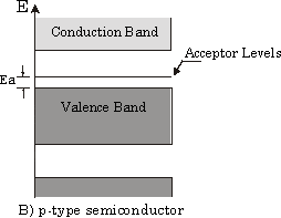
EB5Q3qmELlL1-TdBsC1ySoEOCaieNF-SKt5TiyZzK8rTuQlrMyb6KFOOCiM1388xhuBraQXGThzv3IezIIVvyll82rI9pdGg.gif


I thought the above explanation is either wrong or counter intuitive.

My own thought:
although Al atoms are injected into the Si lattice, my uneducated guess is that, this block of Si-Al solid probably retained much of the tetrahedral structure, so valence band structure did not change that much compared to a pure block of Si. So the new valence band of Si-Al will have similar width and energy height compared to a valance band of a pure block of Si (for example, if orginal Si's valence band was 10ev high, and 1ev wide, then Si-Al's valance band is probably 9ev high and 0.9ev wide, not much difference)
But now, In Si-Al you will have less total electrons in the solid, so valence Band will have some empty spaces instead of being fully filled, Allowing minority carrier - electron, from other metals or n-types to drop in and recombine. If the recombination is too slow, and you have enough electrons and enough voltage persvasion, even minority carriers can conduct thru the p-type, thus the explanation for npn's pn junction.

If I was right, the the short version of my thought would be: Valence bands of the electrons in Si and Si-Al are similar, but fermi levels of electrons in Si and Si-Al are different, Si-Al's fermi level is lower due to less electrons. allowing empty valence states to exist
 
Physics news on Phys.org
  • #2
Why do you think the explanation offered is wrong/counter intuitive?
 
  • #3
ugenetic said:
From some literature, I read the following band structure of the Al doped Si.
The explanation offered: "have vacant acceptor levels at energy Ea above the valence band. Electrons from the top of the valence band can be easily excited into these levels."
EB5Q3qmELlL1-TdBsC1ySoEOCaieNF-SKt5TiyZzK8rTuQlrMyb6KFOOCiM1388xhuBraQXGThzv3IezIIVvyll82rI9pdGg.gif


I thought the above explanation is either wrong or counter intuitive.

My own thought:
although Al atoms are injected into the Si lattice, my uneducated guess is that, this block of Si-Al solid probably retained much of the tetrahedral structure, so valence band structure did not change that much compared to a pure block of Si. So the new valence band of Si-Al will have similar width and energy height compared to a valance band of a pure block of Si (for example, if orginal Si's valence band was 10ev high, and 1ev wide, then Si-Al's valance band is probably 9ev high and 0.9ev wide, not much difference)
But now, In Si-Al you will have less total electrons in the solid, so valence Band will have some empty spaces instead of being fully filled, Allowing minority carrier - electron, from other metals or n-types to drop in and recombine. If the recombination is too slow, and you have enough electrons and enough voltage persvasion, even minority carriers can conduct thru the p-type, thus the explanation for npn's pn junction.

If I was right, the the short version of my thought would be: Valence bands of the electrons in Si and Si-Al are similar, but fermi levels of electrons in Si and Si-Al are different, Si-Al's fermi level is lower due to less electrons. allowing empty valence states to exist

This makes very little sense. For example:

for example, if orginal Si's valence band was 10ev high, and 1ev wide, then Si-Al's valance band is probably 9ev high and 0.9ev wide, not much difference

What is this "high" and "wide"? There is no "width" here other than the size of the bands. Are you talking about the entire bandwidth? If you are, then those values are extremely wrong.

But now, In Si-Al you will have less total electrons in the solid, so valence Band will have some empty spaces instead of being fully filled,

If this is true, then this this will conduct even at T=0, since there are already intrinsic vacancies (holes) even in the valence band. Do you think Si-Al compound is a conductor even at that temperature? Because if it is, it is NOT a semiconductor anymore!

Zz.
 
  • #4
the numbers about si or si-Al were made-up, they were examples to explain "high" (closer to 0 potential) and "wide" (how wide is the valence band, in eV). what does this have anything to do with T = 0? at T=0 fermi level falls exactly on the top edge of valence band, and there is no more "50% distribution" about fermi level. every state above fermi energy have 0 chance of seeing an electron, every state below fermi energy have 100% of seeing an electron.

I don't know exact values of fermi energy of a particular mix of Si and Al @ T=0, I don't know what energy is needed to excite electron to free itself from the yoke or Atoms and Lattice. Have not gotten that far yet. But one thing I am certain, a voltage source may not be strong enough to excite electrons to move, a CURRENT source will cause electrons to flow thru.

Anyways, going back to my question
My original post was saying the below:
upload_2015-3-29_16-4-36.png
 

Attachments

  • upload_2015-3-29_15-56-18.png
    upload_2015-3-29_15-56-18.png
    12.5 KB · Views: 707
  • #5
ugenetic said:
the numbers about si or si-Al were made-up, they were examples to explain "high" (closer to 0 potential) and "wide" (how wide is the valence band, in eV). what does this have anything to do with T = 0? at T=0 fermi level falls exactly on the top edge of valence band, and there is no more "50% distribution" about fermi level. every state above fermi energy have 0 chance of seeing an electron, every state below fermi energy have 100% of seeing an electron.

You have a severe misunderstanding here. The Fermi level doesn't change with temperature! It is defined at T=0, and it is NOT exactly at the top edge of the valence band at T=0! For an intrinsic semiconductor, it is ALWAYS in the middle of the gap! For an extrinsic semiconductor, it depends on the density of the dopant!

Other than that, I have no idea what you had written in the rest of your post. I suggest you look at the FULL band structure of Al-doped Si!

Zz.
 
  • #6
Thank you for staying with me, I appreciate your patience. My English is not that good. My motive is not solving academic problems, thus my questions are very odd as well. So thank you.

Now, Fermi level and Fermi energy are two different concepts. Fermi level does vary with temperature, it is the hypothetical 50% level electron fill level. I think your "Fermi level" is referring to "Fermi energy", which is the "T=0, filling up all states and see at what level we end up with" level.

I don't think anyone will re-read any of my post, so could you just comment on the picture with blue and red I posted. in one sentence, "P-type can conduct, because the fermi level (50% chance electrons can fill that level) is very close to the valance band" Or "P-type doesn't have enough electrons to fill up the valance band".
 
Last edited:
  • #7
I think you started with a misconception, a band structure is an energy structure, it represents possible energy levels(each having no. Of possible quantum states) that can be occupied by particles(say electrons), these are formed when wave functions representing neighbouring interacting particles are overlapped.
So, you can safely say that the valance band structure of an intrinsic Si and Al doped Si will be different.
And the explanation that you want to counter i.e. "have vacant acceptor levels at energy Ea above the valence band. Electrons from the top of the valence band can be easily excited into these levels." is absolutely correct.
Well try to think like this, an Al atom has 3 valance electrons and Si has 4, which means there will be an unoccupied hole(since Si needs 4 bonds). The energy state Ea is called the acceptor energy state representing an energy level of these empty positions(acceptor holes), at Ea the quantum states are supposedly to be empty at T=0 (freeze out effect). As Temperature increases the thermal energy is utilized by some of the electrons in the valance band and they get excited to acceptor energy state. Which makes aluminium atoms -ve charges and produces a holes in the valance band, such valance band holes constitutes hole current.

I hope it helps you.
 

1. What is aluminum doped silicon?

Aluminum doped silicon is a type of semiconductor material that has been intentionally modified by adding aluminum to the silicon crystal structure. This process is known as doping and it is used to alter the electrical properties of the material.

2. How does aluminum doping affect the valence band of silicon?

Aluminum doping introduces additional energy levels into the valence band of silicon, which can alter the band structure and thus the electrical conductivity of the material. This can make the material more or less conductive, depending on the amount and type of aluminum doping used.

3. What is the role of holes in aluminum doped silicon?

Holes are the absence of electrons in the valence band of a semiconductor. In aluminum doped silicon, the presence of aluminum atoms creates holes in the valence band, which can contribute to the overall electrical conductivity of the material. These holes can also interact with other dopant atoms or impurities to further modify the material's properties.

4. How is aluminum doped silicon used in electronic devices?

Aluminum doped silicon is commonly used in electronic devices as a semiconductor material, as it can be easily modified to exhibit specific electrical properties. It is used in the production of transistors, diodes, and integrated circuits, among other devices.

5. What are the advantages of using aluminum doped silicon in electronic devices?

There are several advantages to using aluminum doped silicon in electronic devices. It has a high melting point, making it suitable for high-temperature applications. It is also readily available and relatively inexpensive compared to other semiconductor materials. Additionally, aluminum doped silicon can be easily tailored to exhibit specific electrical properties, making it versatile for use in various electronic devices.

Similar threads

  • Atomic and Condensed Matter
Replies
5
Views
1K
  • Atomic and Condensed Matter
Replies
2
Views
2K
  • Atomic and Condensed Matter
Replies
4
Views
2K
  • Atomic and Condensed Matter
Replies
5
Views
4K
  • Atomic and Condensed Matter
Replies
7
Views
2K
  • Atomic and Condensed Matter
Replies
1
Views
4K
Replies
5
Views
6K
  • Atomic and Condensed Matter
Replies
2
Views
2K
Replies
4
Views
4K
  • Atomic and Condensed Matter
Replies
1
Views
2K
Back
Top