- #1
David331
- 31
- 1
- Homework Statement
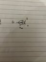
- The gate potential
- Relevant Equations
- ?
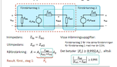
Hi, not really a homework question just a quick question regarding FET-transistor. If the gate potential is -4V does that mean that in the figure below that uGS is -4V. If not, what does it mean and how do you use it in a bigger circuit problem?