A couple of questions about diodes and the depletion region

Click For Summary

Discussion Overview

The discussion revolves around the behavior of diodes, specifically focusing on the depletion region, charge carrier dynamics, and band diagrams in semiconductor physics. Participants explore questions related to the movement of electrons in the context of electric fields and potential energy gradients within diodes.

Discussion Character

  • Exploratory
  • Technical explanation
  • Conceptual clarification
  • Debate/contested

Main Points Raised

  • Some participants question why free electrons in the N side of a diode are not attracted to the positively charged ions in the depletion region.
  • Others discuss the concept of band bending and its relation to potential energy curves, suggesting that this bending creates a built-in electric field in the depletion zone.
  • A participant notes that the conduction band is lower in the N side than in the P side, indicating that more electrons are available to move in the N side.
  • There are inquiries about how a gradient in the potential field leads to the creation of an electric field.
  • One participant emphasizes the importance of understanding the energy levels in semiconductors to grasp the behavior of charge carriers.
  • Another participant expresses frustration over perceived communication barriers in understanding the questions being posed.

Areas of Agreement / Disagreement

Participants do not reach a consensus on the specific mechanisms of charge movement and the implications of band bending. Multiple competing views and uncertainties remain regarding the interpretation of the depletion region and the behavior of charge carriers.

Contextual Notes

Limitations include potential misunderstandings of semiconductor physics concepts, such as the relationship between energy bands and charge carrier dynamics, as well as the implications of electric fields in the depletion region.

Karagoz
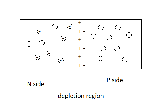
In a diode, we have N side, P side, and a depletion region, made of positive and negative charged sides. N side and P side of the diodes are neutral charge.
Diodes.png


In N side there are free electrons. In the positive charged side of the depletion region, there are positively ionized atoms that "lack" electrons.Why the free electrons at the N side don't get "pulled" to the positive charged part of the depletion region, and neutralize the ionized atoms there?

Or why electrons at the N side don't get pulled by the positive charge of the depletion region?

And in the sunar collectors, how does the "depletion region" causes the "free electrons" on the P side move from P-side to the N-side, when there's a "barrier" of negative charge in the "depletion region" that would push the electrons back to the P side?
 
Last edited by a moderator:
Physics news on Phys.org
Karagoz said:
In a diode, we have N side, P side, and a depletion region, made of positive and negative charged sides. N side and P side of the diodes are neutral charge.
View attachment 213017

In N side there are free electrons. In the positive charged side of the depletion region, there are positively ionized atoms that "lack" electrons.Why the free electrons at the N side don't get "pulled" to the positive charged part of the depletion region, and neutralize the ionized atoms there?

Or why electrons at the N side don't get pulled by the positive charge of the depletion region?

Look at the band diagram in the depletion zone:

3.-Energy-band-diagram-of-a-p-n-junction.jpg


Notice the band-bending. Now, these are equivalent to the "potential energy" curves versus position. Dig back from your E&M class and recall that dV/dx has a significance (hint: it is equivalent to the electric field).

So if the bend bending causes the presence of a built-in electric field in the depletion zone, what do you think will maintain the separation between the positive and negative charge carriers?

Zz.
 
ZapperZ said:
Look at the band diagram in the depletion zone:

View attachment 213021

Notice the band-bending. Now, these are equivalent to the "potential energy" curves versus position. Dig back from your E&M class and recall that dV/dx has a significance (hint: it is equivalent to the electric field).

So if the bend bending causes the presence of a built-in electric field in the depletion zone, what do you think will maintain the separation between the positive and negative charge carriers?

Zz.

How does that band bending cause electric field in the depletion zone?
 
Karagoz said:
How does that band bending cause electric field in the depletion zone?

How does a gradient in the potential field causes an electric field?

Zz.
 
ZapperZ said:
How does a gradient in the potential field causes an electric field?

Zz.

What I only understood from the diagram is that the conduction band is lower in the N side than in the P side. So in the N side more electrons are in the conduction band, thus are "free" to move.
 
Karagoz said:
What I only understood from the diagram is that the conduction band is lower in the N side than in the P side. So in the N side more electrons are in the conduction band, thus are "free" to move.

I wish you’d answer my question.

Zz.
 
ZapperZ said:
I wish you’d answer my question.

Zz.

Yes but I didn't understand the question, and don't know the answer.
 
Karagoz said:
Yes but I didn't understand the question, and don't know the answer.

Then you should have said so, because it tells me at what level of knowledge that you already possessed to be able to understand the answers that you will be receiving. It is why I was asking you such question, because you did not describe what you can understand and what you can't.

The "bend bending" is due to the different "energy levels" of the conduction and valence band in n-type semiconductor and p-type semiconductor. When there is a gradient in the energy band (i.e. the slope of E versus distance is not zero), then there is a "net force" built in due to the contact potential difference between the two material. This is the "culprit" that forces the majority charge carrier of one type to go to one side, while the other type to go to the opposite side. This bend-bending is the SOURCE, the explanation, and the origin, of these charges being pushed to one side. This was why I was asking if you know what a gradient in the potential field leads to.

You will need to learn about band diagram of semiconductors (intrinsic and extrinsic) if you want to know more about how these bands come about.

So next time you ask a question and you get "prodding" responses or questions back, don't ignore them. Someone is trying to figure out what type of answers that you might be capable of understanding. There is no point in giving you the complete answer that you cannot comprehend. It will be a waste of time and effort.

Zz.
 
Last edited:
  • Like
Likes   Reactions: anorlunda
As I know when electrons get energy and excited, they can move from valence band to the conductive band. Electrons at the conductive band are "free". More such "free" electrons in a matter causes the matter to be more "conductive", also easier to move charge through the matter. There are more such "free electrons" in metals than in plastics.

3-energy-band-diagram-of-a-p-n-junction-jpg.jpg


In the pictre above, above Ec is the conductive band, and below Ev is the valence band.

The diagram above shows that the "conductive band" and "valence band" is lower in the N side of the semiconductor than in the P side. That means it requires less energy to get an electron "excited" and move from valence band to the conductive band. And this means there are more free electrons in the N side than in the P side.

This band bending causes the charges being pushed to one side. But how does this band bending cuase charges, electrons and holes, pushed to one or other side?
 

Attachments

  • 3-energy-band-diagram-of-a-p-n-junction-jpg.jpg
    3-energy-band-diagram-of-a-p-n-junction-jpg.jpg
    12.1 KB · Views: 776
  • #10
This is like talking to a wall!

Zz.
 

Similar threads

  • · Replies 2 ·
Replies
2
Views
3K
  • · Replies 1 ·
Replies
1
Views
10K
  • · Replies 8 ·
Replies
8
Views
5K
  • · Replies 3 ·
Replies
3
Views
6K
  • · Replies 20 ·
Replies
20
Views
11K
  • · Replies 2 ·
Replies
2
Views
2K
  • · Replies 1 ·
Replies
1
Views
3K
  • · Replies 5 ·
Replies
5
Views
30K
Replies
3
Views
2K
  • · Replies 12 ·
Replies
12
Views
4K