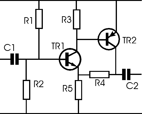
Think of the transistors as voltage controlled resistors. E.G. When there is a voltage between the base and emitter of TR1, the switch starts to turn on (i.e. the resistance between the collector and emitter lowers) and current flows through TR1 from the collector to the emitter. So you have th think about this in terms of Ohm's Law. I.e you have to consider all three variables: current, voltage and resistance.
C1 is an input filter which blocks DC but passes an AC voltage to the base of NPN transistor TR1. R1 and R2 form a voltage divider that generates a fixed DC voltage which DC biases the base of TR1. When an AC signal is applied at the input, the passed AC signal adds with the DC bias voltage and hence the instantaneous voltage at the base of TR1 vibrates up and down around the DC bias voltage.
Then the instantaneous resistance of the collector-emitter path of TR1 changes in sync with the AC signal.
R3, R5, and the instantaneous collector-emitter resistance of TR1 form a second voltage divider circuit. Therefore the voltage at the collector varies as a function of the instantaneous resistance of the collector-emitter path of TR1. Resistors R1, R2, R3 and R5 control the amount of current flowing is both the base-emitter path and the collector-emitter paths of TR1. Typically the values are selected so that more current flows through the collector-emitter path than through the base-emitter path. Hence this circuit is a current amplifier circuit. In voltage terms, we could say that the instantaneous voltage at the collector of TR1 (i.e. the voltage across R3), varies more than the instantaneous voltage at the base.
However, it is also possible to set the values of the resistors to produce a gain of 1. In this case, the current through the collector-emitter of TR1 is higher that the base-emitter current but the voltages are identical. The circuit is purely a current amplifier. This circuit is frequently used to drive transmission lines longer than a few feet by providing more current to the transmission line.
Note that the voltages at the emitter-base and collector-emitter circuit paths are 180 deg. out of phase.
With respect to TR2, remember that it is a PNP transistor. It's resistance is highest when the base-emitter voltage is 0. This occurs when the base is at V+. In the NPN transistor TR1, the base voltage would be 0.
C2 is an output filter that functions exactly as the input filter - the AC signal passes but the DC signal is blocked.
With that info, how about if you try to figure out how TR2 works in this circuit? Think about it, post a response and I will fill in any blanks still left over.
