SUMMARY
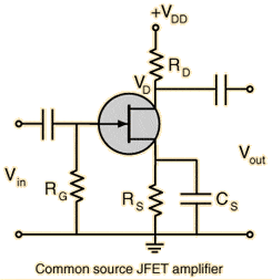
The discussion focuses on the impact of gate resistance (Rg) on JFET amplifier performance. Rg serves as a pull-down resistor that influences the input impedance and gain of the amplifier. It is calculated using the formula Rg = (Vgs / Idss) * (1 - gm * Rl), where Vgs is the gate-source voltage, Idss is the drain-source current at zero gate-source voltage, gm is the transconductance, and Rl is the load resistance. Proper selection of Rg is critical to prevent incorrect bias conditions and ensure optimal signal amplification.
PREREQUISITES
- Understanding of JFET (Junction Field-Effect Transistor) operation
- Familiarity with amplifier circuit design principles
- Knowledge of basic electronic components, including resistors and capacitors
- Ability to calculate transconductance (gm) and load resistance (Rl)
NEXT STEPS
- Study the effects of varying Rg on JFET amplifier gain
- Learn about the role of capacitors in signal coupling and timing
- Explore advanced JFET biasing techniques for improved performance
- Investigate the relationship between input impedance and signal distortion in amplifiers
USEFUL FOR
Electronics engineers, audio engineers, and students studying amplifier design who seek to optimize JFET amplifier performance and understand the significance of gate resistance in circuit applications.
