How to derive a log-antilog opamp square law transfer function?

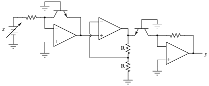
In summary, this is not a homework question. I found a worksheet online with an example of a square law circuit built using log-antilog operational amplifiers. I tried to derive the transfer function but I can't seem to eliminate the reverse saturation current term ##I_S##. I would really appreciate some help with this problem.Assuming all resistors are equal value, all transistors are perfectly matched and at equal temperature and all op-amps are ideal, the circuit would work as follows: The first stage would take the square root of the input signal (y = √x). The second stage would have a gain of 2 and the last stage would have a gain of e (
  • #1
fonz
151
5
TL;DR Summary
log-antilog opamp question
Firstly, this is not a homework question. I found a worksheet online with an example of a square law circuit built using log-antilog operational amplifiers. I tried to derive the transfer function but I can't seem to eliminate the reverse saturation current term ##I_S##. I would really appreciate some help with this problem.
I have included the schematic below:
01019x01.png


Here is my attempt:

Assuming all resistors are equal value, all transistors are perfectly matched and at equal temperature and all op-amps are ideal.

Output of first stage:

##V_{O1} = - V_T ln(\frac{V_{IN}}{R I_S})##

Output of second stage:

##V_{O2}= 2V_{O1}##

Output of third stage:

##V_{O3} = - RI_Se^{\frac{V_{O2}}{V_T}}##

Sub 1 into 2:

##V_{O2} = -2V_Tln(\frac{V_{IN}}{RI_S}) = - V_Tln(\frac{V_{IN}^2}{R^2I_S^2})##

Sub into 3:

##V_{O3} = - RI_Se^{-ln(\frac{V_{IN}^2}{R^2I_S^2})} = -RI_S\frac{R^2I_S^2}{V_{IN}^2} = - \frac{R^3I_S^3}{V_{IN}^2}##
 
Engineering news on Phys.org
  • #2
It looks as if Is is just a constant, a characteristic of the transistor, which we must have to define the characteristic.
 
  • #3
Is is the saturation current of the diode and it is a physical property of the device just like the resistance of the resistor. https://en.wikipedia.org/wiki/Saturation_current Usually one DC biases the diode (or the BE's PN junction in this case) at a couple of operating points and then curve fits to the schottky diode equation to get it.

BTW, Is it usual to make a log and anti-log amplifier by using the virtual short of the op amp to keep the NPN's BC off? (i.e. base is ground, collector is virtual ground) I guess the opamp is usually compensated to be very slow (10s of KHz) so it's probably 6-to-one half dozen to the other but it seems like just shorting BC with a wire is a safer way to make a diode from a BJT. I am wondering if anyone knows the pro/con of grounding the base in a log amplifier. Maybe the turn on properties are better?
 
  • Like
Likes fonz
  • #4
Hi thanks for the replies. I probably should have been clearer in my original post. I am asking whether I have derived the correct transfer function for this circuit not what the reverse saturation current is in relation to the operation of a BJT.

Thanks
 
  • #5
Looks right to me and it passes the sniff test because -Exp[-2Ln(x)]=-1/(x^2).

Why do you think you need to eliminate Is?

In this circuit the BJT is masquerading as a diode because V(BC)=0. Is is just an intrinsic property of that diode just like R is an intrinsic property of the resistor.
 
  • Like
Likes fonz
  • #6
Hi thanks for the reply. I found the problem on the link below, the question suggests the transfer function should simply by the square of the input but my derivation suggests that it isn't which is why I was doubtful.

https://www.allaboutcircuits.com/worksheets/nonlinear-opamp-circuits/

Thanks again
 
  • #7
You mean question 7 right? As an analog engineer, I read "This circuit takes the square root of the input signal (y = √x)." as the output of the circuit is proportional to Sqrt[x] but we could also just play a tricky game. Choosing R=1/Is -> y=Sqrt[x]
 
  • Like
Likes fonz
  • #8
Hi thanks again for the reply. It was Question 8 I attempted.
 
  • #9
Actually, now that I think about it the transfer function given for question 8 is wrong. The middle stage should be inverting.

If the middle stage had G=-2 then y=-x^2=-Exp[-2(-Ln[x])] when R=1/Is. (One can also measure x in units of Vt and ignore it.)

With the non-inverting middle stage the transfer function is the one you found.

1/x^2 and x^2 very different functions and there is no proportionality constant that will make them the same.

P.S. Question 7 should also have G=-1/2, not 1/2, to give y=Sqrt[x]
 
  • Like
Likes fonz
  • #10
If for simplicity we assumed that the first stage output is -In(x) and the second stage gain is 2 and the last stage gain is e(x) we have y = e^( -In(x)*2 ) = 1/(x^2). Of course, the first and the last stage are not ideal they add offset (Is*R) but this is normal.
 
  • Like
Likes fonz
  • #11
Thanks forthe replies. I thought that ##I_S## was an incredibly small number, something like ##10^{-9}## which would mean that unless the resistance was huge the output would be really small.
 
  • #12
fonz said:
unless the resistance was huge the output would be really small.

That's just because the model we're using for the diode is overly simplistic. Here is a simple example with a better model. It compares the output of gain curve of the log amp to the ideal function when the resistor is 1Meg using a standard diode.

% cat log.sp
*
E1 y 0 0 n 10K
R1 n x 1Meg
X1 n y 1N4148
V1 x 0 PWL(0 0 1 1)
******************************************
*NXP Semiconductors
.SUBCKT 1N4148 1 2
*
* The resistor R1 does not reflect
* a physical device. Instead it
* improves modeling in the reverse
* mode of operation.
*
R1 1 2 5.827E+9
D1 1 2 1N4148
*
.MODEL 1N4148 D
+ IS = 4.352E-9
+ N = 1.906
+ BV = 110
+ IBV = 0.0001
+ RS = 0.6458
+ CJO = 7.048E-13
+ VJ = 0.869
+ M = 0.03
+ FC = 0.5
+ TT = 3.48E-9
.ENDS
.tran 100m 1
.print tran v(y) exp(-v(x))
.end
% ngspice -b log.sp # note: for this simulation v(x)=t so the tran is also drawing the gain curve.
--------------------------------------------------------------------------------
Index time v(y) exp(-v(x))
--------------------------------------------------------------------------------
0 0.000000e+00 -9.64830e-13 1.000000e+00
1 1.000000e-04 -1.03575e-03 9.999000e-01
2 2.000000e-04 -2.12523e-03 9.998000e-01
3 4.000000e-04 -4.24671e-03 9.996001e-01
...
13 1.056000e-01 -1.59227e-01 8.997845e-01
14 1.256000e-01 -1.67437e-01 8.819676e-01
15 1.456000e-01 -1.74477e-01 8.645034e-01
...
39 6.256000e-01 -2.45224e-01 5.349404e-01
40 6.456000e-01 -2.46765e-01 5.243478e-01
41 6.656000e-01 -2.48259e-01 5.139651e-01
...
57 9.856000e-01 -2.67507e-01 3.732152e-01
58 1.000000e+00 -2.68219e-01 3.678794e-01
 
  • Like
Likes fonz

FAQ: How to derive a log-antilog opamp square law transfer function?

1. What is a log-antilog opamp square law transfer function?

A log-antilog opamp square law transfer function is a mathematical expression that describes the relationship between the input and output of an operational amplifier (opamp) circuit. It is commonly used in electronic design to model the behavior of opamp circuits in various applications.

2. How do you derive a log-antilog opamp square law transfer function?

The derivation of a log-antilog opamp square law transfer function involves using the properties of logarithms and exponents to manipulate the equations that describe the behavior of an opamp circuit. This typically requires a strong understanding of algebra and circuit analysis techniques.

3. What are the key components of a log-antilog opamp square law transfer function?

The key components of a log-antilog opamp square law transfer function include the input voltage, the opamp gain, and the output voltage. Additionally, the function may also include other parameters such as bias currents and resistor values, depending on the specific circuit being analyzed.

4. Can a log-antilog opamp square law transfer function be used to design opamp circuits?

Yes, a log-antilog opamp square law transfer function can be used to design opamp circuits. By understanding the behavior of the function and how it relates to the physical components of an opamp circuit, engineers can use it to design circuits that meet specific performance requirements.

5. Are there any limitations to using a log-antilog opamp square law transfer function?

While a log-antilog opamp square law transfer function can be a useful tool in designing opamp circuits, it does have some limitations. For example, it may not accurately model the behavior of non-ideal components in a circuit, such as noise or temperature effects. Additionally, it may not be suitable for more complex circuit designs that involve multiple opamps or feedback loops.

Similar threads

Back
Top