cabraham
- 1,181
- 90
BJT is ultimately charge controlled. The following terminal equations are used to describe bjt:
Ic = beta*Ib
Ic = Ies *exp ((Vbe/Vt) - 1)
Ic = alpha * Ie
A good simulation program or lab tests will affirm that changes in current happen before change in voltage. A p-n junction has some capacitance, as well as inductance. At the frequencies the bjt operates at, capacitance dominates. The *Vbe* cannot change unless *charge* is injected into the b-e junction in the form of base & emitter currents, Ib & Ie. As soon as Ie changes, Ic changes a moment later, then Vbe eventually "catches up".
The easiest way to see this is to observe a simulation of a signal diode, such as a 1N914B, or 1N4148.
A simulation is attached. Notice how current exhibits the stair case function, while voltage gradually rises to reach the new value. The diodes voltage is determined by its current, not vice-versa.
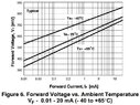
An i-v graph of the 1N914B diode is attached. The Vbe "barrier value" depends on forward current. At 10 uA current, Vbe is just under 0.40 volt at room temp.
The Shockley diode equation simply describes the relation between I & V. It can be written 2 ways:
1) Is = Is * exp ((Vd/Vt) - 1),
2) Vd = Vt * ln ((Id/Is) + 1).
Just as Id = f(Vd), Vd = f(Id).
For further study, please search using these terms:
Diode reverse recovery
Diode forward recovery.
Finally, we can discuss *Early effect.* it is true that collector current is *slightly influenced* by Vce, collector emitter voltage, but this is relatively small. A 20% increase in Ie results in about a 20% increase in Ic.
But a 20% increase in Vce results in an Ic change *much less* than 20%.
To claim that the bjt is slightly "voltage controlled by Early effect" is not wrong. The key word here is "slightly".
Ic = beta*Ib
Ic = Ies *exp ((Vbe/Vt) - 1)
Ic = alpha * Ie
A good simulation program or lab tests will affirm that changes in current happen before change in voltage. A p-n junction has some capacitance, as well as inductance. At the frequencies the bjt operates at, capacitance dominates. The *Vbe* cannot change unless *charge* is injected into the b-e junction in the form of base & emitter currents, Ib & Ie. As soon as Ie changes, Ic changes a moment later, then Vbe eventually "catches up".
The easiest way to see this is to observe a simulation of a signal diode, such as a 1N914B, or 1N4148.
A simulation is attached. Notice how current exhibits the stair case function, while voltage gradually rises to reach the new value. The diodes voltage is determined by its current, not vice-versa.
An i-v graph of the 1N914B diode is attached. The Vbe "barrier value" depends on forward current. At 10 uA current, Vbe is just under 0.40 volt at room temp.
The Shockley diode equation simply describes the relation between I & V. It can be written 2 ways:
1) Is = Is * exp ((Vd/Vt) - 1),
2) Vd = Vt * ln ((Id/Is) + 1).
Just as Id = f(Vd), Vd = f(Id).
For further study, please search using these terms:
Diode reverse recovery
Diode forward recovery.
Finally, we can discuss *Early effect.* it is true that collector current is *slightly influenced* by Vce, collector emitter voltage, but this is relatively small. A 20% increase in Ie results in about a 20% increase in Ic.
But a 20% increase in Vce results in an Ic change *much less* than 20%.
To claim that the bjt is slightly "voltage controlled by Early effect" is not wrong. The key word here is "slightly".