brainbaby
- 232
- 5
Hi friends,
I have simulated two circuits, one is an RC filter and other is a Capacitance multiplier.
My aim of experiment is to validate a decrease in Iout (load current) of CM circuit as compared to load current in RC filter circuit.
Theoretically,
Iout (CM circuit) < Iout (RC filter)
Vp-p (CM circuit) < Vp-p (RC filter)
My results:
1.RC filter
Vout (dc) = 0.0458716 ( .op 300ms)
Iout (dc) = 0.00458716
Vout (ac) = 43.7 ~ 48 mV (.tran 300ms)
Iout (ac) = 4.80 ~ 4.37 mA
Vp-p (ripple) = 0.00437018 (.meas)
2.CM circuit
Vout (dc) = 0.323751
Iout (dc) = 0.0323751
Vout (ac) = 322 ~ 327 mV
Iout (ac) = 32.65 ~ 32.15 ma
Vp-p (ripple) = 0.00521016 (.meas)
From the above results its quite clear that implementing CM circuit causes Iout to increase which particularly against the aim of the CM circuit. As the CM circuit works by decreasing the load current which according to load POV can be visualised as increase in capacitance.
We can also see the peak to peak ripple voltage in both the circuits, Vp-p for CM circuit should be less than Vp-p ripple of an RC filter, but again the simulations results are quite opposite.
What's wrong here??
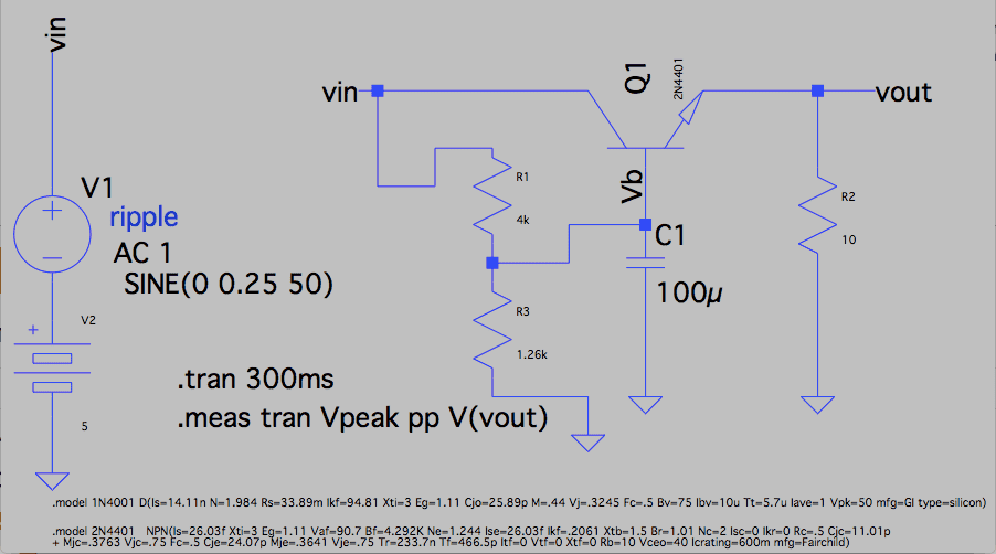
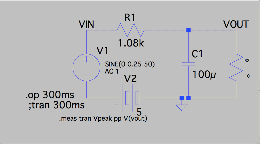
I have simulated two circuits, one is an RC filter and other is a Capacitance multiplier.
My aim of experiment is to validate a decrease in Iout (load current) of CM circuit as compared to load current in RC filter circuit.
Theoretically,
Iout (CM circuit) < Iout (RC filter)
Vp-p (CM circuit) < Vp-p (RC filter)
My results:
1.RC filter
Vout (dc) = 0.0458716 ( .op 300ms)
Iout (dc) = 0.00458716
Vout (ac) = 43.7 ~ 48 mV (.tran 300ms)
Iout (ac) = 4.80 ~ 4.37 mA
Vp-p (ripple) = 0.00437018 (.meas)
2.CM circuit
Vout (dc) = 0.323751
Iout (dc) = 0.0323751
Vout (ac) = 322 ~ 327 mV
Iout (ac) = 32.65 ~ 32.15 ma
Vp-p (ripple) = 0.00521016 (.meas)
From the above results its quite clear that implementing CM circuit causes Iout to increase which particularly against the aim of the CM circuit. As the CM circuit works by decreasing the load current which according to load POV can be visualised as increase in capacitance.
We can also see the peak to peak ripple voltage in both the circuits, Vp-p for CM circuit should be less than Vp-p ripple of an RC filter, but again the simulations results are quite opposite.
What's wrong here??
Attachments