hayowazzup
- 63
- 0
Hello, I am currently working on a PCB design project,
just wondering if anybody knows how to reduce the size of the gap(the black circular region) around individual pin of IC Chips (after I have done the polygon pour)
so that a 0.5mm ground track can get through.
In addition, what is the minimum size that I could reduce it down to? does that depend on the "pcb board printer"?
unfortunately I cannot upload the image for now
but here is an example involving ic chips
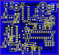
just wondering if anybody knows how to reduce the size of the gap(the black circular region) around individual pin of IC Chips (after I have done the polygon pour)
so that a 0.5mm ground track can get through.
In addition, what is the minimum size that I could reduce it down to? does that depend on the "pcb board printer"?
unfortunately I cannot upload the image for now
but here is an example involving ic chips
Last edited: