What is Op amp: Definition and 307 Discussions
An operational amplifier (often op amp or opamp) is a DC-coupled high-gain electronic voltage amplifier with a differential input and, usually, a single-ended output. In this configuration, an op amp produces an output potential (relative to circuit ground) that is typically 100,000 times larger than the potential difference between its input terminals. Operational amplifiers had their origins in analog computers, where they were used to perform mathematical operations in linear, non-linear, and frequency-dependent circuits.
The popularity of the op amp as a building block in analog circuits is due to its versatility. By using negative feedback, the characteristics of an op-amp circuit, its gain, input and output impedance, bandwidth etc. are determined by external components and have little dependence on temperature coefficients or engineering tolerance in the op amp itself.
Op amps are used widely in electronic devices today, including a vast array of consumer, industrial, and scientific devices. Many standard IC op amps cost only a few cents; however, some integrated or hybrid operational amplifiers with special performance specifications may cost over US$100 in small quantities. Op amps may be packaged as components or used as elements of more complex integrated circuits.
The op amp is one type of differential amplifier. Other types of differential amplifier include the fully differential amplifier (similar to the op amp, but with two outputs), the instrumentation amplifier (usually built from three op amps), the isolation amplifier (similar to the instrumentation amplifier, but with tolerance to common-mode voltages that would destroy an ordinary op amp), and negative-feedback amplifier (usually built from one or more op amps and a resistive feedback network).
View More On Wikipedia.org
-

Engineering Analyzing this operational amplifier circuit with DC
Hi all, I attached my attempt at a solution in the attached picture. I am using the textbook titiled as ”electronic circuit analysis“ by David E. Johnson, and op amp is in chap 3; while I did not find any example that attach the Vee and Vcc with amplifier . It seems that v+ = v- doesn’t hold in...- ZoeDale
- Thread
- Replies: 8
- Forum: Engineering and Comp Sci Homework Help
-
U
How to Calculate the Complex Op Amp in Circuit Diagram
TL;DR Summary: How to calculate the operational amplifiers in the circuit diagram Hello Everyone, I am trying to learn the circuit diagram of one of a device in which I will be doing modifications as a part of my Masters's Research to make it performance better. My background is in Mechanical...- umair1998
- Thread
- Replies: 8
- Forum: Engineering and Comp Sci Homework Help
-

Optimizing an Op Amp Current Sense Circuit: Are the Calculations Correct?
TL;DR Summary: Trying to solve the op amp current sense circuit as per the schematic. I want to solve the below current sense op amp circuit, Are the calculations correct? As of now i modified the circuit by removing the capacitors, i will add them once the above circuit calculations are...- PhysicsTest
- Thread
- Replies: 21
- Forum: Engineering and Comp Sci Homework Help
-

Calculating the voltage in an OP-amp circuit with a current source
Summary:: Find the voltage in an OP-amp circuit with current source I(in) = 1 uA. What I'm confused about is if there is any voltage flowing through R1. Because if there was and let's say it went downwards, then where would it go, I mean it cannot just disappear. And if it goes upwards...- DenDanne
- Thread
- Replies: 1
- Forum: Engineering and Comp Sci Homework Help
-

Engineering Why is a differential amplifier considered the same as a subtractor?
So after using superposition and setting the ratio R2/R1 = R4/R3 the same or R2=R4 and R1=R3,i come to the eq. for output voltage Vout= R2/R1 * (V2-V1) or R4/R3(V2-V1). And in the book foundations of analog and digital electronics by agarwal and lang, they are saying that this circuit is a...- altruan23
- Thread
- Replies: 1
- Forum: Engineering and Comp Sci Homework Help
-
Engineering Opamp adder circuit: Where does the "-" come from?
So i used KCL and both currents are flowing into the node, and then leaving together to go to the resistor R3. So my eq can be seen in the picture. I was looking in a book and they had a minus infront of the parantheses. Is the current flowing from R3 into the node??- altruan23
- Thread
- Replies: 8
- Forum: Engineering and Comp Sci Homework Help
-
Engineering OPamp circuit - how to simplify this term?
So this is the circuit. And here i tried to calculate Uout/ Uin , any suggestion how to simplify this term?? I used Uout= Uin * (1+ Z2/Z1)- altruan23
- Thread
- Replies: 2
- Forum: Engineering and Comp Sci Homework Help
-
Engineering Op amp circuit -- Did I calculate the output voltage correctly?
can someone check, if i calculated the output voltage correct? i used virtual ground because V+-input of the op amp is 0 --> V- input is then also 0.- altruan23
- Thread
- Replies: 12
- Forum: Engineering and Comp Sci Homework Help
-
A
Inverting op amp frequency response Bode plot help
Using analog discovery 2 kit and the bode plot produced by the network analyzer is off. The scope looks fine and everything is behaving how it should except for the bode plot. The magnitude of the bode plot will start at the correct dB then right before tapering off it shoots up a few dB and...- alvogel122
- Thread
- Replies: 13
- Forum: Electrical Engineering
-
E
This op amp does not have gain?
Had this as a question from a class mate. This op amp should not have any gain in the DC or AC circuit. The coupling cap blocks DC and has no reference to get gain, while the AC needs a cap in the feedback loop to get gain. Is that correct? Oh, this is supposed to be in the inverting configuration.- EENSEEY
- Thread
- Replies: 4
- Forum: Electrical Engineering
-

Amplifier for piezoelectric sensor, OP Amp circuit
Hello everyone ! I'm working with a piezoelectric cell and I need to retrieve the variation of the charge of the cell as a voltage signal. I found this circuit (a charge amplifier) with an OP Amp ( here the piezo cell is represented as the current source with the capacitor and the resistor on...- hugo_faurand
- Thread
- Replies: 6
- Forum: Electrical Engineering
-

Operational Amplifiers & Resistors to form a Black Box
So basically I am trying to give an output of Vo = 10(V2-V1) From Figure 9 Example Gain of first Op Amp = Rf / R1, if R1 & R2 are equal. What's throwing me off is using 5 resistors to create a circuit rather than 6 or just 3. My initial thoughts were the following: To use the first loop...- Jason-Li
- Thread
- Replies: 10
- Forum: Introductory Physics Homework Help
-
M
Noninverting op amp doesn't work on a highly resistive load
Hi, I am using an Apex PA443DF operational amplifier to drive a sinusoidal signal at 100 V amplitude across a very large resistor with resistance of about 5000 Mega ohms. The amplifiers are set up as noninverting with a gain of 22 and function very well for small resistive loads. The sinusoids...- mlamont1
- Thread
-
- Tags
- Amp High voltage Load Op amp Work
- Replies: 31
- Forum: Electrical Engineering
-
J
Engineering Sketching output waveforms while considering slew rate
1. Using the frequency equation I know the time period is 1 millisecond. 2. The duty cycle (50%) equation tells me that the pulse width and the amplitude is 1 V. 3. Thus the input waveform looks like this : (?) 4. As the slew rate is 0.5 volts per microsecond, the output voltage would take...- JC2000
- Thread
-
- Tags
- Electronics Op amp Output Rate Waveforms
- Replies: 3
- Forum: Engineering and Comp Sci Homework Help
-
J
Engineering Basic opamp design problem ##V_{output} = 3V_1 - 2V_2##
Here I let ##R_2 = 2 ## kohms and ##R_1 = 1## kohms. Using this suggests that ##R_3 = 0## and ## R_4 = 1 ## kohms (?!) The resulting circuit is Is this the correct way to solve this? PS : I just realized that I have interchanged ##V_1## and ## V_2## in the diagram!- JC2000
- Thread
-
- Tags
- Design Electronics Op amp Opamp
- Replies: 12
- Forum: Engineering and Comp Sci Homework Help
-

Engineering How can I find the open loop voltage gain of this opamp?
The open loop voltage gain is given as : $$ u(s) = \frac{u_o}{1+\frac{s}{w_o}} = \frac{100}{1 + \frac{s}{40}}$$ Where u_o is the d.c. voltage gain and w_o is the pole. The op amp that is given is: And I am told to use the non ideal op amp model as follows: Well my guess is that I can find the...- Boltzman Oscillation
- Thread
- Replies: 9
- Forum: Engineering and Comp Sci Homework Help
-
N
Operational Amplifier key parameters
<< Mentor Note -- new poster has been reminded to show their work on schoolwork-type problems >>- nobodyhere
- Thread
- Replies: 2
- Forum: Introductory Physics Homework Help
-
Engineering Op Amp Books: Gain, Feedback & Examples
I was wanting to get a book on Op Amps. Ideally it would have lots of examples but I also need it to explain gain, feedback, and all that important material in an understandable manner.- Boltzman Oscillation
- Thread
- Replies: 9
- Forum: Science and Math Textbooks
-
D
Confusion on: High Pass Filter at Op Amp Input
Hello, I am simulating the input impedance of a high-pass filter with the output voltage of the filter input to the non-inverting pin of an op amp. I'm confused as to why the input impedance can possibly dip below the resistance of the high-pass filter resistor. Please see the following circuit...- decaf14
- Thread
- Replies: 6
- Forum: Electrical Engineering
-
D
I have an op amp that does not tolerate signals below ground
I have a lm224 operational amplifier that does not tolerate signals below ground. What operational amplifier tolerates signals below ground?- David lopez
- Thread
- Replies: 13
- Forum: Electrical Engineering
-

Design of an Op Amp Circuit for Voltage Amplification
Hi Everyone, I would like to measure voltage output from a sensor via an Arduino. The sensor outputs 20 mV at max capacity. I'd like to bump this up to around 5 volts so it is easier to measure. My plan was to use a non-inverting topology coupled with an LM393N op-amp. The schematic for a...- runningman19
- Thread
- Replies: 9
- Forum: Electrical Engineering
-

Engineering Circuit input impedance with ground in an OP Amp circuit
I've been given the following circuit and have been asked to find the input impedance and the impedance between the input terminal and ground. I've never encountered an operational amplifier configured like this. I know that the voltages at the - and + terminals of the op amp are ideally equal...- bobg123
- Thread
- Replies: 4
- Forum: Engineering and Comp Sci Homework Help
-
What is the gain error for this opamp driven by a voltage
Homework Statement The op amp has a near ideal level 1 model with G = 5000V/V, ri = inf, ro = 0 How would I obtain the feedback function? Homework Equations I know I have to find the feedback function which is: f = - (ΔV/Vin) The Attempt at a Solution I will first drive using the...- Boltzman Oscillation
- Thread
- Replies: 18
- Forum: Engineering and Comp Sci Homework Help
-
Engineering Derive expressions for the voltage gain of this opamp circuit
Homework Statement Derive the expressions for the voltage gain (Gv) of the following op amp: Homework Equations In = Ip = 0 Vp =VnThe Attempt at a Solution I can use KCL, and the fact that In and Ip are both 0, to derive the two equations, one from the top node and the other from the...- Boltzman Oscillation
- Thread
- Replies: 11
- Forum: Engineering and Comp Sci Homework Help
-
How can I analyze this transimpedance amplifier?
Homework Statement The opAmp network shown in figure 68 is a transimpedance amplifer that employs both negative and positive feedback. Assuming that the op-amp is ideal, calculate the value for the output voltage for Jg is 1mA.The circuit and question are this...- Boltzman Oscillation
- Thread
- Replies: 13
- Forum: Engineering and Comp Sci Homework Help
-
W
Charging a battery and monitoring the current w/ an instrumentation amp
Homework Statement Homework Equations CMRR = Av/Acm Acm= Δ/R , Δ = (2 x Tolerance of Resistor).R The Attempt at a Solution I have to admit I am a bit confused by the premise of the problem. My understanding is Vout is used to vary Vcharge in some way, so that Icharge is always 1.3 A. Then...- Weaver
- Thread
- Replies: 7
- Forum: Engineering and Comp Sci Homework Help
-
W
Instrumentation op-amp problem
Homework Statement Homework Equations [/B] CMRR = Av/Acm Acm= Δ/R , Δ = (2 x Tolerance of Resistor).R The Attempt at a Solution I have an issue with part e) and f) but here are all my workings c) For this part, Acm would be: 10 x10^-3 This makes 2.5mV -> 0.25 uV (which is the same...- Weaver
- Thread
-
- Tags
- Instrumentation Op amp Op-amp
- Replies: 1
- Forum: Engineering and Comp Sci Homework Help
-
E
Op Amp Vout Calculation for Non-Inverting Configuration
Homework Statement Solve for Vout Homework Equations Vout=Vin(1+Rf/R) The Attempt at a Solution I get it is a non-inverting op amp but there is no resistor from the non-inverting terminal to the output. I have no idea how the equation would be. I understand that noninverting is...- esob
- Thread
- Replies: 4
- Forum: Engineering and Comp Sci Homework Help
-
E
How to solve for Vout of this op amp
How would you solve for Vout? I get it is a non-inverting op amp but there is no resistor from the noninverting terminal to the output.- esob
- Thread
- Replies: 3
- Forum: Electrical Engineering
-
W
Engineering Grounding Op-Amp circuit exercise
Homework Statement 2. Homework Equations 3. The Attempt at a Solution For the first set of questions: I've worked through to part 6), at which is I encountered my first problem. I'm not entirely sure what the question is asking. Is it as if there would be a capacitor between... -

What happens when you flip the inputs of an op amp?
So, from my textbook, and what seems to be standard, an inverting amplifier circuit goes something like this: However, when I switch the terminals of the op amp and follow through with the equations, I get the same Vout. So my question then is what is the difference? I know there is other...- Abdullah Almosalami
- Thread
- Replies: 78
- Forum: Electrical Engineering
-

Hi, i need to know if this DAC-op-amp calculation is ok
Homework Statement Homework EquationsThe Attempt at a Solution- NYAME EPHRAIM
- Thread
- Replies: 5
- Forum: Engineering and Comp Sci Homework Help
-
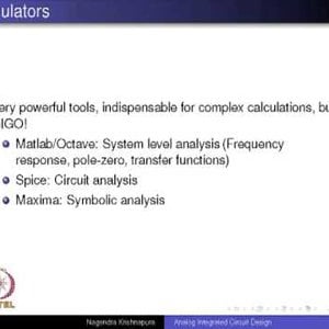
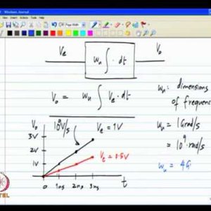
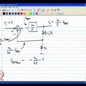
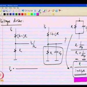
Analog IC Design by Dr. Nagendra Krishnapura (NPTEL):- Course introduction; Negative feedback control
COPYRIGHT strictly reserved to Prof. Dr. Nagendra Krishnapura and NPTEL, Govt. of India. Duplication Prohibited. Lectures: http://www.nptel.ac.in/courses/117106030/ Syllabus: http://www.nptel.ac.in/syllabus/syllabus.php?subjectId=117106030- Wrichik Basu
- Media item
- analog electrical ic design iit kharagpur op amp
- Comments: 0
- Category: Engineering
-
Analog IC Design by Dr. Nagendra Krishnapura (NPTEL):- Negative feedback amplifier
COPYRIGHT strictly reserved to Prof. Dr. Nagendra Krishnapura and NPTEL, Govt. of India. Duplication Prohibited. Lectures: http://www.nptel.ac.in/courses/117106030/ Syllabus: http://www.nptel.ac.in/syllabus/syllabus.php?subjectId=117106030- Wrichik Basu
- Media item
- analog electrical ic design iit kharagpur op amp
- Comments: 0
- Category: Engineering
-
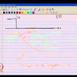
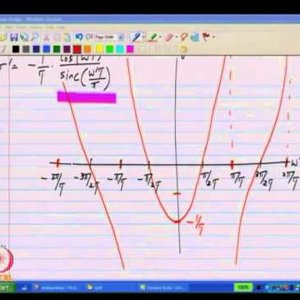
Analog IC Design by Dr. Nagendra Krishnapura (NPTEL):- Step response, sinusoidal steady state response
COPYRIGHT strictly reserved to Prof. Dr. Nagendra Krishnapura and NPTEL, Govt. of India. Duplication Prohibited. Lectures: http://www.nptel.ac.in/courses/117106030/ Syllabus: http://www.nptel.ac.in/syllabus/syllabus.php?subjectId=117106030- Wrichik Basu
- Media item
- analog electrical ic design iit kharagpur op amp
- Comments: 0
- Category: Engineering
-
Analog IC Design by Dr. Nagendra Krishnapura (NPTEL):- Loop gain and unity loop gain frequency; Opamp
COPYRIGHT strictly reserved to Prof. Dr. Nagendra Krishnapura and NPTEL, Govt. of India. Duplication Prohibited. Lectures: http://www.nptel.ac.in/courses/117106030/ Syllabus: http://www.nptel.ac.in/syllabus/syllabus.php?subjectId=117106030- Wrichik Basu
- Media item
- analog electrical ic design iit kharagpur op amp
- Comments: 0
- Category: Engineering
-
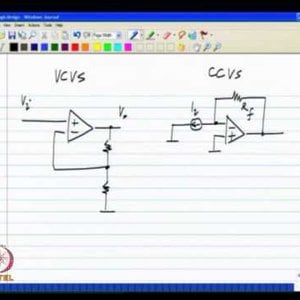
Analog IC Design by Dr. Nagendra Krishnapura (NPTEL):- Opamp realization using controlled sources; Delay in the loop
COPYRIGHT strictly reserved to Prof. Dr. Nagendra Krishnapura and NPTEL, Govt. of India. Duplication Prohibited. Lectures: http://www.nptel.ac.in/courses/117106030/ Syllabus: http://www.nptel.ac.in/syllabus/syllabus.php?subjectId=117106030- Wrichik Basu
- Media item
- analog electrical ic design iit kharagpur op amp
- Comments: 0
- Category: Engineering
-
Analog IC Design by Dr. Nagendra Krishnapura (NPTEL):- Negative feedback amplifier with ideal delay-small delays
COPYRIGHT strictly reserved to Prof. Dr. Nagendra Krishnapura and NPTEL, Govt. of India. Duplication Prohibited. Lectures: http://www.nptel.ac.in/courses/117106030/ Syllabus: http://www.nptel.ac.in/syllabus/syllabus.php?subjectId=117106030- Wrichik Basu
- Media item
- analog electrical ic design iit kharagpur op amp
- Comments: 0
- Category: Engineering
-
Analog IC Design by Dr. Nagendra Krishnapura (NPTEL):- Negative feedback amplifier with ideal delay-large delays
COPYRIGHT strictly reserved to Prof. Dr. Nagendra Krishnapura and NPTEL, Govt. of India. Duplication Prohibited. Lectures: http://www.nptel.ac.in/courses/117106030/ Syllabus: http://www.nptel.ac.in/syllabus/syllabus.php?subjectId=117106030- Wrichik Basu
- Media item
- analog electrical ic design iit kharagpur op amp
- Comments: 0
- Category: Engineering
-
Analog IC Design by Dr. Nagendra Krishnapura (NPTEL):- Negative feedback amplifier with parasitic poles and zeros
COPYRIGHT strictly reserved to Prof. Dr. Nagendra Krishnapura and NPTEL, Govt. of India. Duplication Prohibited. Lectures: http://www.nptel.ac.in/courses/117106030/ Syllabus: http://www.nptel.ac.in/syllabus/syllabus.php?subjectId=117106030- Wrichik Basu
- Media item
- analog electrical ic design iit kharagpur op amp
- Comments: 0
- Category: Engineering
-
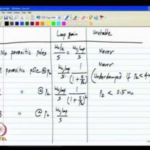
Analog IC Design by Dr. Nagendra Krishnapura (NPTEL):- Negative feedback amplifier with parasitic poles and zeros; Nyquist criterion
COPYRIGHT strictly reserved to Prof. Dr. Nagendra Krishnapura and NPTEL, Govt. of India. Duplication Prohibited. Lectures: http://www.nptel.ac.in/courses/117106030/ Syllabus: http://www.nptel.ac.in/syllabus/syllabus.php?subjectId=117106030- Wrichik Basu
- Media item
- analog electrical ic design iit kharagpur op amp
- Comments: 0
- Category: Engineering
-
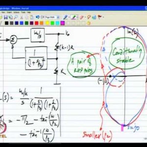
Analog IC Design by Dr. Nagendra Krishnapura (NPTEL):- Nyquist criterion; Phase margin
COPYRIGHT strictly reserved to Prof. Dr. Nagendra Krishnapura and NPTEL, Govt. of India. Duplication Prohibited. Lectures: http://www.nptel.ac.in/courses/117106030/ Syllabus: http://www.nptel.ac.in/syllabus/syllabus.php?subjectId=117106030- Wrichik Basu
- Media item
- analog electrical ic design iit kharagpur op amp
- Comments: 0
- Category: Engineering
-
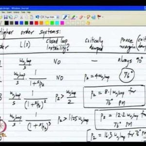
Analog IC Design by Dr. Nagendra Krishnapura (NPTEL):- Phase margin
COPYRIGHT strictly reserved to Prof. Dr. Nagendra Krishnapura and NPTEL, Govt. of India. Duplication Prohibited. Lectures: http://www.nptel.ac.in/courses/117106030/ Syllabus: http://www.nptel.ac.in/syllabus/syllabus.php?subjectId=117106030- Wrichik Basu
- Media item
- analog electrical ic design iit kharagpur op amp
- Comments: 0
- Category: Engineering
-
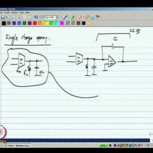
Analog IC Design by Dr. Nagendra Krishnapura (NPTEL):- Single stage opamp realization
COPYRIGHT strictly reserved to Prof. Dr. Nagendra Krishnapura and NPTEL, Govt. of India. Duplication Prohibited. Lectures: http://www.nptel.ac.in/courses/117106030/ Syllabus: http://www.nptel.ac.in/syllabus/syllabus.php?subjectId=117106030- Wrichik Basu
- Media item
- analog electrical ic design iit kharagpur op amp
- Comments: 0
- Category: Engineering
-
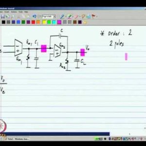
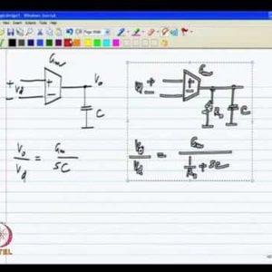
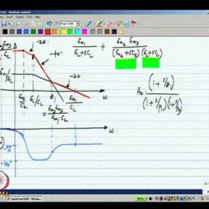
Analog IC Design by Dr. Nagendra Krishnapura (NPTEL):- Two stage miller compensated opamp - 1
COPYRIGHT strictly reserved to Prof. Dr. Nagendra Krishnapura and NPTEL, Govt. of India. Duplication Prohibited. Lectures: http://www.nptel.ac.in/courses/117106030/ Syllabus: http://www.nptel.ac.in/syllabus/syllabus.php?subjectId=117106030- Wrichik Basu
- Media item
- analog electrical ic design iit kharagpur op amp
- Comments: 0
- Category: Engineering
-
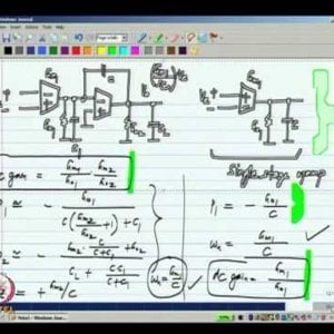
Analog IC Design by Dr. Nagendra Krishnapura (NPTEL):- Two stage miller compensated opamp - 2
COPYRIGHT strictly reserved to Prof. Dr. Nagendra Krishnapura and NPTEL, Govt. of India. Duplication Prohibited. Lectures: http://www.nptel.ac.in/courses/117106030/ Syllabus: http://www.nptel.ac.in/syllabus/syllabus.php?subjectId=117106030- Wrichik Basu
- Media item
- analog electrical ic design iit kharagpur op amp
- Comments: 0
- Category: Engineering
-
Analog IC Design by Dr. Nagendra Krishnapura (NPTEL):- Two and three stage miller compensated opamps; Feedforward compensated opamp - 1
COPYRIGHT strictly reserved to Prof. Dr. Nagendra Krishnapura and NPTEL, Govt. of India. Duplication Prohibited. Lectures: http://www.nptel.ac.in/courses/117106030/ Syllabus: http://www.nptel.ac.in/syllabus/syllabus.php?subjectId=117106030- Wrichik Basu
- Media item
- analog electrical ic design iit kharagpur op amp
- Comments: 0
- Category: Engineering
-
Analog IC Design by Dr. Nagendra Krishnapura (NPTEL):- Feedforward compensated opamp - 2
COPYRIGHT strictly reserved to Prof. Dr. Nagendra Krishnapura and NPTEL, Govt. of India. Duplication Prohibited. Lectures: http://www.nptel.ac.in/courses/117106030/ Syllabus: http://www.nptel.ac.in/syllabus/syllabus.php?subjectId=117106030- Wrichik Basu
- Media item
- analog electrical ic design iit kharagpur op amp
- Comments: 0
- Category: Engineering
-
Analog IC Design by Dr. Nagendra Krishnapura (NPTEL):- Feedforward compensated opamp - 3
COPYRIGHT strictly reserved to Prof. Dr. Nagendra Krishnapura and NPTEL, Govt. of India. Duplication Prohibited. Lectures: http://www.nptel.ac.in/courses/117106030/ Syllabus: http://www.nptel.ac.in/syllabus/syllabus.php?subjectId=117106030- Wrichik Basu
- Media item
- analog electrical ic design iit kharagpur op amp
- Comments: 0
- Category: Engineering
-

Analog IC Design by Dr. Nagendra Krishnapura (NPTEL):- Feedforward compensated opamp - 4; typical opamp data sheet
COPYRIGHT strictly reserved to Prof. Dr. Nagendra Krishnapura and NPTEL, Govt. of India. Duplication Prohibited. Lectures: http://www.nptel.ac.in/courses/117106030/ Syllabus: http://www.nptel.ac.in/syllabus/syllabus.php?subjectId=117106030- Wrichik Basu
- Media item
- analog electrical ic design iit kharagpur op amp
- Comments: 0
- Category: Engineering