Circuit Analysis Question (Truth Table, Logic etc.)

In summary: AB'C'D'In summary, the question asks how to find a logic circuit given an equation and the person is having difficulty understanding how to draw the circuit. They found a video online that explained how to draw the circuit from the equation.
  • #1
jisbon
476
30
Homework Statement
-
Relevant Equations
-
Hi all,
Having some problems digesting on electric circuits. Below is an example of a question and I would like to ask how do I go ahead in solving this.

Firstly, for these types of questions:
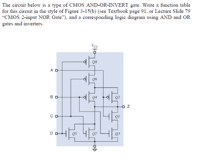
1586675162072.png


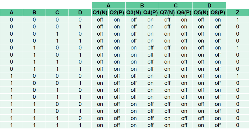
I have understood how to write a function table, and it goes something like this:
1586675202811.png

Now what I am having problems with is constructing the equation and the logic circuit. I searched online and found that the equation is simply the sum of all the variables that will give a HIGH, which in this case, is z = A'B'C'D' + A'BC'D' + AB'C'D'
Is this correct?

If it is, how do I then determine how the logic circuit should be drawn? I'm pretty confused on how do I even start one.As for the second question, it is simply (I guess a reverse) of the above question. It tells me to design a CMOS circuit given an equation:
1586693950209.png


I managed to derive the logic circuit based on the equation, which is:
1586675409344.png


Now,how do I draw the CMOS circuit? Quite overwhelmed :/

Anyone who can refer me to some videos/reading materials on this would be great. I don't understand how do I simply draw one :/

Thanks!
 

Attachments

  • 1586675383393.png
    1586675383393.png
    5.6 KB · Views: 165
Last edited by a moderator:
Physics news on Phys.org
  • #2
jisbon said:
I searched online and found that the equation is simply the sum of all the variables that will give a HIGH, which in this case, is z = A'B'C'D' + A'BC'D' + AB'C'D'
Is this correct?
I didn't check that logic but it's probably correct. The important thing to me is that you didn't see the obvious alternate expression (C'D') * NOT(AB) [had to use "NOT" cause I haven't learned Latex. It's important to look for patterns and this one just jumps right out at you if you are at all used to looking. Also, I think that expression is more amenable to a simpler circuit.
 
  • #3
phinds said:
I didn't check that logic but it's probably correct. The important thing to me is that you didn't see the obvious alternate expression (C'D') * NOT(AB) [had to use "NOT" cause I haven't learned Latex. It's important to look for patterns and this one just jumps right out at you if you are at all used to looking. Also, I think that expression is more amenable to a simpler circuit.
True, if it is (C'D') * NOT(AB), how do I draw out the logic circuit though?
 
  • #4
jisbon said:
True, if it is (C'D') * NOT(AB), how do I draw out the logic circuit though?
Well, with the simplest logic elements (NOT necessarily the simplest logic circuit) you would just do EXACTLY what the equation says: put C and D into inverters and the output into an AND gate, and so forth. If you want to use more realistic NAND gates it takes a few seconds of extra thought.
 
  • #5
phinds said:
Well, with the simplest logic elements (NOT necessarily the simplest logic circuit) you would just do EXACTLY what the equation says: put C and D into inverters and the output into an AND gate, and so forth. If you want to use more realistic NAND gates it takes a few seconds of extra thought.
Ok, I'm not exactly sure how does one draws the logic circuit from the equation, but I will try my best to understand you.

So, in this case, both C and D are inverse. So maybe something like this?
1586696355387.png

Wouldn't it be like (C'D')+(A..B..) ? I'm not exactly sure of how can one 'derive' the logic circuit?
 
  • #6
I don't want to give the answer, but it's exactly the same approach you used for the second problem. I'm going to simply copy and paste what you had in the original post and draw a few arrows to emphasize what each part of the equation meant in terms of schematic logic.

approach.png


The CMOS circuit by the way is practically solved here. Say for instance you know what an inverter circuit is. Do you see right after A you have an inverter here? Replace the inverter with the lower level circuitry that uses transistors instead for your CMOS version of it. The OR followed by a NOT is very convenient because NOR is two less transistors than an OR and it's probably in your textbook. The only "trickier" one is the AND because your textbook probably shows you how to do a NAND, but you can copy your textbook NAND and follow directly behind it an inverter for AND.

Again: I don't want to give you the answer so I'll show you the approach for another classic circuit called a multiplexer (MUX). I just did this on the fly so apologies for some scribbles and potential error although the intention is to share the approach or recipe for solving a "hard" problem in small easier steps.

mux example.jpg


By the way I've heard the MUX is a common interview question.
 
  • #7
Ok, I redid some stuff and here's my attempt:
z = A'B'C'D' + A'BC'D' + AB'C'D'
= (C'D') * (A'B'+A'B+AB')
= (C'D') * (B'(A'+A)+A'B)
= (C'D') * (B'+A'B) since a+bc=(a+b)(a+c)...
= (C'D') * (A'+A)(A'+B')
= (C'D') * (A'+B')
1586747857108.png


Something like this?
 
  • #8
Note that ##A' B' \neq (AB)'##
 
  • #9
jisbon said:
Ok, I redid some stuff and here's my attempt:
z = A'B'C'D' + A'BC'D' + AB'C'D'
= (C'D') * (A'B'+A'B+AB')
= (C'D') * (B'(A'+A)+A'B)
= (C'D') * (B'+A'B) since a+bc=(a+b)(a+c)...
= (C'D') * (A'+A)(A'+B')
= (C'D') * (A'+B')
When you get used to this stuff you will just write down the last line of the above, not the first line at all, because it is so obvious, except that as has been pointed out, you have the A'+B' wrong. Just look at the truth table and look at what I already told you.
 
  • #10
phinds said:
When you get used to this stuff you will just write down the last line of the above, not the first line at all, because it is so obvious, except that as has been pointed out, you have the A'+B' wrong. Just look at the truth table and look at what I already told you.
I'm new at this though :/

Joshy said:
Note that ##A' B' \neq (AB)'##
Ok, I think I figured out. (ab)' = a'+b'
a'b' = (a+b)'
So, for (C'D') * (A'+B')
1586749191184.png
 
  • #11
@jibson if you are not already intimitately familiar with DeMorgan's Theorems (which are EXTREMELY simple), you will find them to be probably the single most useful thing to know regarding these kinds of logic circuit and truth table analysis. With them you would not have made the mistake you made.
 
  • #12
If you don't mind me asking... which class are you taking? What's the textbook? Is this an Introduction to Digital Design type of class? I saw part of the question asked for a CMOS equivalent. I'm asking because I am curious about what the likely expectation might be.
 
  • #13
Joshy said:
If you don't mind me asking... which class are you taking? What's the textbook? Is this an Introduction to Digital Design type of class? I saw part of the question asked for a CMOS equivalent. I'm asking because I am curious about what the likely expectation might be.
Yep, it's my first time dealing with this kind of stuff and so, it's an introductory module to digital circuits. The recommended textbook was Digital Designs, Principles and Practices (although I think not all information was taught in there)

On a second note, was the updated diagram correct? Thanks so much
 
  • Like
Likes Joshy
  • #14
phinds said:
@jibson if you are not already intimitately familiar with DeMorgan's Theorems (which are EXTREMELY simple), you will find them to be probably the single most useful thing to know regarding these kinds of logic circuit and truth table analysis. With them you would not have made the mistake you made.
Yep, trying to learn it at the moment, thanks for the feedback
 
  • #15
Learning is okay.

I was worried when I saw the CMOS question. That is usually pretty advanced more for like an IC design class that involves layout, but it doesn't sound like you'll be covering that... very interesting in my personal opinion, that the author brings it up so early into the book.

Stick with solving small problems first and wiring it up into its bigger system just like you did in your last posts. You're making progress :)

DeMorgan's is super helpful. Great job with using it. Now that you've wired up your circuit there's a simple way for you to check if it worked. The best thing about a class like this is you can more easily check on your own if the answer is correct. Try plugging in values for A, B, C, and D and see if gives you what you expect:

check.jpg


You can check all of them, which would be recommended if it's homework and/or if you're not feeling confident with your solution. If you're in an exam you can spot check a few points and check the rest after you've finished the exam and if you have enough time. The first one I checked for you looks like it matches the table so far; the answer doesn't look outrageous to me.
 
  • Like
Likes jisbon
  • #16
Joshy said:
Learning is okay.

I was worried when I saw the CMOS question. That is usually pretty advanced more for like an IC design class that involves layout, but it doesn't sound like you'll be covering that... very interesting in my personal opinion, that the author brings it up so early into the book.

Stick with solving small problems first and wiring it up into its bigger system just like you did in your last posts. You're making progress :)

DeMorgan's is super helpful. Great job with using it. Now that you've wired up your circuit there's a simple way for you to check if it worked. The best thing about a class like this is you can more easily check on your own if the answer is correct. Try plugging in values for A, B, C, and D and see if gives you what you expect:

View attachment 260536

You can check all of them, which would be recommended if it's homework and/or if you're not feeling confident with your solution. If you're in an exam you can spot check a few points and check the rest after you've finished the exam and if you have enough time. The first one I checked for you looks like it matches the table so far; the answer doesn't look outrageous to me.
Hmm.. In this case, I'm kind of sure my answer is correct, but from the solution I have gotten from my friends, it appears that the last part of the circuit is wrong where just before the output, instead of a AND, it's a OR. So I'm kind of stuck I guess?
 
  • #17
I just tried it with another test case to see just before that last AND if it should have been an OR.

OR I know if the inputs are 1 or 0, then the output is 1. AND the input are 1 and 0, then the output is 0. Let's try to get inputs like these into your last AND.

I tried ##A=0##, ##B=1##, ##C=1##, and ##D=1##. This makes the top one with the NAND become a 1; the bottom NOR becomes a 0. Now the input to my AND is 1 and 0, which has the output of a 0. I took a look at the table and that seems to work with the table so far. If you immediately swapped the AND for an OR you'd be in trouble.

Run through your truth table.

edit:

They may have taken advantage of DeMorgan's. My professor called it "pushing the bubble." The output of your first two has that bubble. Remember what you did when you had ##A'B' = (A+B)'##? Maybe the logic circuits they have on the first stage is a AND and OR after "pushing the bubble?" There are multiple ways to solve the circuit. Personally if I were going to draw the CMOS for these circuits then I'd rather have the NAND (4 transistors) and NOR (4 transistors) compared to AND (6 transistors) and OR (6 transistors).
 
  • #18
Joshy said:
I just tried it with another test case to see just before that last AND if it should have been an OR.

OR I know if the inputs are 1 or 0, then the output is 1. AND the input are 1 and 0, then the output is 0. Let's try to get inputs like these into your last AND.

I tried ##A=0##, ##B=1##, ##C=1##, and ##D=1##. This makes the top one with the NAND become a 1; the bottom NOR becomes a 0. Now the input to my AND is 1 and 0, which has the output of a 0. I took a look at the table and that seems to work with the table so far. If you immediately swapped the AND for an OR you'd be in trouble.

Run through your truth table.

edit:

They may have taken advantage of DeMorgan's. My professor called it "pushing the bubble." The output of your first two has that bubble. Remember what you did when you had ##A'B' = (A+B)'##? Maybe the logic circuits they have on the first stage is a AND and OR after "pushing the bubble?" There are multiple ways to solve the circuit. Personally if I were going to draw the CMOS for these circuits then I'd rather have the NAND (4 transistors) and NOR (4 transistors) compared to AND (6 transistors) and OR (6 transistors).
Just ran through, so it seems that the answer key is wrong? :H

This is the answer key:
1586759611098.png
 
  • #19
No. It's the same as your answer. They pushed the bubble (DeMorgan's), which was what I was trying to talk about in that last piece.

See the OR gate at the back followed by the NOT? Let's say those two intermediate nodes are X and Y. Then you've got ##(X+Y)'=Z##, right? Remember DeMorgan's? ##(X+Y)'=X'Y'##. Now it's an AND with two NOTS into the input (##X'## and ##Y'##). Keep going from right to left move those NOTs to the end of the first circuits and you've got exactly what you had. If you ran through the truth table for this circuit you'd see that the answers are the same.
 
  • #20
Oh.. ok.. I think I probably got this for now. Another question is about DeMorgan's: there's this function I'm trying to simplify:
z= c'd'+c'd+a'b'cd+cd'
So as follows,
z = c'(d'+d)+a'b'cd+cd'
= c'+a'b'cd+cd'
=(c'+d')+a'b'cd since (c'+cd')=(c'+c)(c'+d')=(c'+d')
= (cd)' + a'b'cd

Now, I'm pretty sure one can still simplify this, but I'm kind of stuck at this step :/

Also, regarding drawing a CMOS circuit out of a logic circuit, how does one proceed with that? (it's my next question)

Thanks
 
  • #21
I drew an example in post #6, but I'm sure you'll find the circuits in your book. Get the CMOS equivalent for an inverterter (NOT), NAND, and NORs. The circuit schematic you've drawn with the big symbols or shapes you can replace them with the transistor version of it step by step- do it in small sections and wire it up together at the end. I would do it for version of the circuit you have because NAND and NOR uses less transistors than AND and OR.

I can't tell just from looking at it, but you can add some of the old terms you eliminated to use it and reduce other terms. For example ##A = A + A## so if you think have a ##C'D## might be helpful in reducing ##A'B'CD## you could give it a try. If you've learned about k-maps that might be another approach get the answer very quickly and see if you got the minimum.

edit:

There's another one called the consensus theorem that's a bit tricky, but I'll often use it to eliminate terms that didn't matter. It's multiplying the possibly redundant terms with ##X' + X## it's just the same as times ##1##. The clue for using it is when you see one term with the ##X## and the other term with a ##X'## then the third term that doesn't have any ##X## or ##X'## in it you can try multiplying it with ##(X' + X)##.
 

1. What is a truth table in circuit analysis?

A truth table is a visual representation of the possible input combinations and their corresponding outputs in a logic circuit. It is used to determine the logical function of a circuit and to identify any errors or inconsistencies.

2. How do you create a truth table for a logic circuit?

To create a truth table, you first need to identify the number of inputs and outputs in the circuit. Then, list all possible input combinations in binary form. Next, use the circuit diagram to determine the output for each input combination. Finally, organize the inputs and outputs in a table format, with the inputs on the left and the corresponding outputs on the right.

3. What is the purpose of circuit analysis in electronics?

The purpose of circuit analysis is to understand the behavior of electronic circuits and to design and troubleshoot them. It involves using mathematical and logical techniques to analyze the flow of electricity and to determine the function and performance of a circuit.

4. What is the difference between combinational and sequential logic circuits?

Combinational logic circuits have outputs that only depend on the current input values, while sequential logic circuits have outputs that depend on both the current input values and the previous input values. Sequential circuits also have memory elements, such as flip-flops, which allow them to store and manipulate data.

5. How do you simplify a logic circuit using Boolean algebra?

To simplify a logic circuit, you can use Boolean algebra to reduce the number of logic gates and inputs needed. This involves using Boolean identities, such as De Morgan's laws and distributive laws, to manipulate the logic expressions and eliminate redundant gates. The goal is to reduce the complexity and improve the efficiency of the circuit.

Similar threads

  • Engineering and Comp Sci Homework Help
Replies
7
Views
911
Replies
5
Views
2K
  • Engineering and Comp Sci Homework Help
Replies
8
Views
1K
  • Engineering and Comp Sci Homework Help
Replies
10
Views
2K
  • Engineering and Comp Sci Homework Help
Replies
4
Views
3K
  • Engineering and Comp Sci Homework Help
Replies
2
Views
1K
  • Engineering and Comp Sci Homework Help
Replies
5
Views
3K
  • Set Theory, Logic, Probability, Statistics
2
Replies
45
Views
3K
  • Engineering and Comp Sci Homework Help
Replies
9
Views
1K
  • Engineering and Comp Sci Homework Help
Replies
6
Views
776
Back
Top