Effects of emitter capacitor in the BJT CE amplifiers

In summary, the CE amplifier has a voltage gain of Re' / Rc. The input resistance is strongly effected.
  • #1
Clear Mind
38
3
Suppose to have a BJT Common Emitter amplifier like the one below:
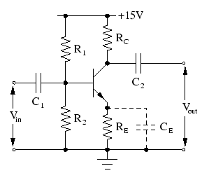
img119.gif

Now, if we send a signal ##V_{in}## with a frequency belonging to the midband frequency interval, we can consider ##C_1, C_2,## and ##C_E## as short circuit. Questions are:

1) What is the effect of ##C_E## (excluding its role on the frequency respond of the amp)?

2) It is right to say that the gain of this amplifier with ##C_E## is:
##A_v=-g_mR_C##
and the gain without ##C_E## is:
##A_v=\frac{-g_mR_C}{1+g_mR_E}##

3) Does the presence of ##C_E## change the values of ##R_{in}## and ##R_{out}##?
 
Engineering news on Phys.org
  • #2
Voltage gain of a CE amplifier with an emitter bypass capacitor is Re' / Rc. Re' is the AC resistance of the base-emitter junction. Zin of a CE amplifier with an emitter bypass capacitor is lower than without. I believe it is Re' / beta all in parallel with the voltage divider network on the base. A properly designed CE voltage amplifier will not be affected much by the variations in transistor beta within the manufacturers beta spec.
 
  • #3
@2) Yes - your answer 2) is 100% correct (The above mentioned expression Re´/Rc is false).
@3) r,out remains , practically, uneffected (please use small letters for dynamic resistances).
And - yes - the input resistance is strongly effected.
At the base node (without R1||R2) the input resistance is r,in=h11+h21*Re.
(in other terms: h11=hie and h21=beta).
In case Re is bypassed by Ce we have only r,in=h11 (applies for frequencies which make 1/wCe very low).
 
  • #4
LvW said:
@2) Yes - your answer 2) is 100% correct.
So we can affirm that (for small signal model) when ##C_E## is present the amplifier behave like a common emitter amplifier without ##R_e##. While if we remove ##C_E##, the amplifier behave like a common emitter with a emitter resistance ##R_e##?
 
  • #5
Clear Mind said:
So we can affirm that (for small signal model) when ##C_E## is present the amplifier behave like a common emitter amplifier without ##R_e##. While if we remove ##C_E##, the amplifier behave like a common emitter with a emitter resistance ##R_e##?

Yep! :smile:
 
  • #6
Clear Mind said:
So we can affirm that (for small signal model) when ##C_E## is present the amplifier behave like a common emitter amplifier without ##R_e##. While if we remove ##C_E##, the amplifier behave like a common emitter with a emitter resistance ##R_e##?
Yes -of course. However, only for frequencies which are large enough to make the capacitive resistance sufficiently small .
 
  • Like
Likes berkeman
  • #7
There is a rapid means of calculating Re:

A handy value to remember is 26 ohms / ma. With a grounded base, and 1 ma through the emitter, the impedance at the emitter will be roughly 26 ohms for a small signal. 52 ohms for .5ma, 13 ohms for 2ma... For derivation, take the derivative of the diode equation...

Next, you have the effective impedance seen from the base. Zbase is R1||R2||Zin, where Zin is most likely dominate. At the emitter, this value will appear to be Zbase / (Beta +1).

Finally, CE is often an electrolytic capacitor with a significant Equivalent Series Resistance of it's own - i.e 10 ohms, .5 ohms for low ESR types.

So, your approximation of Re is:

(Ie / 26 ohms) + ( R1||R2||Zin / (B+1) ) + ESR.

As an example, a transistor with a 50 ohm signal generator, C1 very large, an emitter current of 1 ma, and a typical capacitor ESR of 10 ohm, and a Beta of 100 would see:

26 ohms + 50/101 ohms + 10 ohms = 36.5 ohms.

Note that I ignored R1 and R2 as they're typically much larger than the 50 ohms of the signal generator...0

With Spice interfaces being so common, it is fun to try this with one regular, and one low ESR capacitor and 2-3 emitter currents to provide confidence and intuition.

I quickly modeled it to find the peak-peak output across a 1k collector resistor and found the following:

CE = 1000uf, 10ohm, Ie = 1ma
Predicted: Av = 27.4 Result: 27.2

CE = 1000uf, 10ohm, Ie = .5ma
Predicted: Av = 16.0 Result: 15.9

CE = 1000uf, 0.5 ohm, Ie = 1ma
Predicted: Av = 37.0 Result: 36.6

- Mike
 
  • #8
Averagesupernova said:
Voltage gain of a CE amplifier with an emitter bypass capacitor is Re' / Rc. Re' is the AC resistance of the base-emitter junction. Zin of a CE amplifier with an emitter bypass capacitor is lower than without. I believe it is Re' / beta all in parallel with the voltage divider network on the base. A properly designed CE voltage amplifier will not be affected much by the variations in transistor beta within the manufacturers beta spec.
My bad. I should have said Rc / Re'. This link: http://www.electronics-tutorials.ws/amplifier/amp_2.html explains this CE amp. Never really thought about multiplying by the reciprocal of Re'. Always just divided Rc by Re'. Suspect some folks in this thread are mistaking Re' for Re. Re is the emitter resistor and Re' is pronounced Re prime.
Edit: Ugh! I seem to be off a bit today. Input impedance is Re' * beta all in parallel with the voltage divider network on the base.
 
Last edited:
  • #9
It's funny because I learned the tricks of these circuits while getting an associates, and my bachelor's program was woefully ignorant of the details. That was a cause for a about 2-3 labs to be repeated under supervision to demonstrate I was not cheating.
 
Last edited:
  • #10
Mike_In_Plano said:
There is a rapid means of calculating Re:
A handy value to remember is 26 ohms / ma. With a grounded base, and 1 ma through the emitter, the impedance at the emitter will be roughly 26 ohms for a small signal. 52 ohms for .5ma, 13 ohms for 2ma... For derivation, take the derivative of the diode equation...
- Mike
Hi Mike, I am afraid that you have mixed some things.
In the given circuit RE is an external ohmic resitor in the feedback path providing dc stabilization (negative dc feedback).
You are speaking about another resistance which is NOT an ohmic external part but an INTERNAL effect within the BJT - the transconductance gm=Ic/Vt.
However, only in common base configuration the input resistance at the emitter node is 1/gm=Vt/Ic and some people use the identity 1/gm=r,e.
Note that it is necessary to use small letters for r,e because it is not an ohmic quantitty but a DYNAMIC (differential) parameter.
(Vt is the "thermal voltage" with a value of app. 26mV at room temperature)
 
  • #11
Averagesupernova said:
My bad. I should have said Rc / Re'. .

But we should keep in mind that this expression is a rather rough approximation only. What happens for Re´=0 (No Re or shorted with a capacitor?).
Is the gain infinite? No - the correct equation is given in post#1 under point 2).
 
  • #12
Thanks for the answers guys, you all make my day!

LvW said:
You are speaking about another resistance which is NOT an ohmic external part but an INTERNAL effect within the BJT - the transconductance gm=Ic/Vt.
I saw that you were discussing about internal resistance of the base. You can easily calculate the base resistance using the ##\pi##-hybrid or the ##T## model of BJT, they are both correct and their usance depends on the situation. For instance, when you have ##C_E## you should use the ##\pi##-hybrid model, contrariwise if you take away ##C_E## you should use the ##T## model.

For the ##\pi##-hybrid model the internal base resistance is:
##r_{\pi}=\frac{\beta}{g_m}##

200px-Bipolar_hybrid-pi_model.PNG


while for the ##T## model you get:
##r_e=\frac{\alpha}{g_m}##
(where ##\alpha=\frac{\beta}{\beta+1}\approx 1##)

t_model_1.jpg
 
  • #13
Clear Mind said:
I saw that you were discussing about internal resistance of the base.
No - I didn`t.
I spoke about an "internal effect", which - unfortunately - sometimes is called "internal resistor" which is somewhat misleading.

The situation is as follows: We have an input-output transfer characteristik - the curve Ic=f(Vbe) with the typical exponential form.
The slope of this curve is the transconductance gm=d(Ic)/d(Vbe).
This transconductance value appears in the classic voltage gain formula (see post#1).
Here the gain formula can be written as: Av=-Rc/(1/gm+Re).

This formula allows to replace the expression (1/gm) by a "fictive" quantity (in ohms): r,e=1/gm, which - formally - is correct.
But it is not correct to interprete this expression as an existing resistance within the BJT - and, in particular, not as a "resistance of the base".
It is easy to see why it is NOT a resistance because - as mentioned above - it is 1/gm=r,e=d(Vbe)/d(Ic) .
Hence, it connects two quantities which do not share a common path: Vbe and Ic.
This cannot result in any resistance and, therefore, gm is not called "conductance" but "transconductance".

More than that, I do not understand the "T-model" of the BJT.
From this, I derive the relationship r.e=Vbe/Ie what is simply wrong.
 
Last edited:
  • #14
LvW said:
More than that, I do not understand the "T-model" of the BJT.
From this, I derive the relationship r.e=Vbe/Ie what is simply wrong.
Everything is OK. In fact your r,e = 1/gm is incorrect.
Because re is nothing more than a small signal resistance.
re - small signal resistance between base and emitter looking into the emitter.

re = d(Vbe)/d(Ie) = Vt/Ie

and since gm = Ic/Vt

and Ic = alpha*Ie = (β/(β + 1))*Ie we get

gm = Ic/Vt = Ic/Ie * Ie/Vt = Ic/Ie * 1/re = = α*1/re = β/(β+1)*1/re

Also we can use small-signal T model to find out the voltage gain.

attachment.php?attachmentid=62114&stc=1&d=1379977014.png


So we have

Vout = - alpha*Ie*Rc and Vin = Ie*re

So next we have

Av = Vout/Vin = (- alpha*Ie*Rc)/(Ie*re) = Rc/re * alpha = Rc/re * β/(β + 1) ≈Rc/re

Also notice that some professors use Rpi = d(Vbe)/d(Ib) instead of re.

Rpi = (β + 1)*re

Av = (β*Rc)/Rpi = (β*Rc)/( (β + 1)*re) = Rc/re * β/(β + 1) looks familiar ?
 
Last edited:
  • #15
Jony130 said:
Everything is OK. In fact your r,e = 1/gm is incorrect.
Because re is nothing more than a small signal resistance.
re - small signal resistance between base and emitter looking into the emitter.

Hi Joni130
I am happy to agree with you (up to 95%).
However, please note that I did not recommend to set r,e=1/gm - because it is, indeed, NOT any physical resistance between two nodes.
And that is the reason for the remaining 5% of my non-agreement:

I think that r,e is NOT the "signal resistance between base and emitter looking into the emitter."
Instead, it is the input resistance in common base configuration - looking into the emitter.
And this is a remarkable difference - and the reason for my saying that the shown T-model is not correct.
If it would be the signal resistance between B and E, we should have the same current through the B and the E node.
And - as you know - this is not the case. In contrary, both currents show a very large difference.
As another argument, if 1/gm would be the B-E resistance we would have the same value also for common emitter configuration.
(We have a similar situation for the MILLER effect: The effective resistance between the base node and the collector node is, of course, not identical to the external resistor RB between B and C because the current through RB does not consist of the input voltage driven input current only.)

Further comment: In your calculation you define
(a) r,e=Vt/Ie and
(b) r,e=Vin/Ie.

Looks like a contradiction, does it not?
 
Last edited:
  • #16
Last edited:
  • #17
Joni, I did nothing else than to quote two equations from your post, which are contradictory. How can you say "no"?
 
  • #18
Say and do whatever you like on both sides of the argument but the simple fact is that the approximate gain of the CE transistor with an emitter bypass cap IS RC / Re'. In the link I provided it is explained that Re' is .025 volts / emitter current. I always thought of it as an AC resistance of a base-emitter junction but this is probably not technically true. Also, Re' can never get to zero by its very own definition. I am not sure what you are referring to LvW when you say there is no emitter resistor or if it is bypassed with a cap. Re' is STILL there and non-zero. And please forgive me I sometimes get some lower case letters in where they should be caps. :)
-
Edit: Almost forgot. Re' is multiplied by beta to get what I recall being referred to as ZinBase. This would be the impedance of the base without the biasing resistors. Pretty much tells us that it is not really affecting the base at all. It is all about the emitter. Hence it is always included with any emitter resistance when computing voltage gain of a CE amplifier. However, sometimes it is very small compared to other emitter resistance(s) so it can be ignored in those cases.
 
Last edited:
  • #19
This thread has become an embarrassment. It has gone from being an exploration tool to a rude confrontation over who knows what.

Yes, actual mistakes have been made, such as my own trans-conductance as a function of Ie vs Ic.
But arguing over such trivialities as what is implied by Re when the multiple posts gave the definition as Re = dVbe/dIe is to substitute conceptual communication with ego-driven regurgitation.

I suggest we either lock the post or restrict our arguments to those that may be derived.
Furthermore, let's behave as gentlemen. When the nature of argument is apparent, let's not argue over semantics.
 
  • #20
Averagesupernova said:
Re' is STILL there and non-zero. And please forgive me I sometimes get some lower case letters in where they should be caps. :)
In contrary - you should use lower case letters rather than caps!. Let me explain

As far as my person is concerned - this was the reason for a misunderstanding:
When you were writing "Re" I have assumed you were referring to the external resistor in the emitter path because there are many persons using the approximation gain=-Rc/Re" for a gain stage with Re-feedback. Now I have noticed that you were speaking about the transconductance gm=Ic/Vt. And some people prefer to use the inverse form r,e=1/gm. I strongly dislike this form because - as I have mentioned before - r,e is NOT a resistance!.
And the problem (and the cause of a misunderstanding) was that you even have used capital letters (Re) for this dynamic (differential) quantity. Hence, I was of the opinion you are speaking about the feedback resistor. OK?
 
  • #21
Mike_In_Plano said:
This thread has become an embarrassment. It has gone from being an exploration tool to a rude confrontation over who knows what.
.
... rude confrontation? Do you really think so? From which side?
I`ve got the impression that there was a misunderstanding (perhaps only on my side?) because of some "problematic" ways for using symbols. For my opinion, it is really necessary in electronics to distinguish between dynamic and static resistances - otherwise some confusions and misunderstandings cannot be avoided.
And this applies - as we have seen - in particular to transistor circuits which are strongly non-linear circuits. Hence, we always have a mixture between dynamic and static resistors (Re and re).
I hope you believe me that it never was my intention to "embarras" somebody - to me, it was a discussion about equivalent circuits and their interpretation, gain formulas and approxinations, nothing else. And such a discussion is no surprise, because - as you know - there are different explanations how a transistor works and different formulas (more or less exact). Do you know what I mean?
 
  • #22
LvW. Yep. It's all good. Conversely I should sometimes use lower case when I use caps. I referred to the collector resistor as Rc at one point which is incorrect I suspect. I learned to divide the collector resistor by the Re' so that is the way I prefer to do it instead of 1/gm. Neither way is incorrect of course.
 
  • #23
OK - fine.
As an additional problem: From the beginning I did not recognize the "superscript" in the symbol Re´. So it really was not easy to distinguish between Re, Re´, re and r,e.
(I am afraid, the same did happen while reading post#16 from joni130. Only now I have recognized that suddenly one of the diff.resistances have such a superscript: re´instead of re.)
 

1. What is an emitter capacitor in a BJT CE amplifier?

An emitter capacitor is a capacitor that is connected between the emitter and ground in a BJT (bipolar junction transistor) CE (common-emitter) amplifier. It is used to bypass the emitter resistor and provide negative feedback, which helps to stabilize the amplifier's gain and frequency response.

2. How does an emitter capacitor affect the gain of a BJT CE amplifier?

The emitter capacitor helps to stabilize the DC operating point of the transistor by reducing the effect of variations in the base-emitter voltage. This results in a more consistent gain for the amplifier. Additionally, the capacitor also acts as a low-pass filter, reducing high-frequency signals and further improving the amplifier's gain stability.

3. Can an emitter capacitor improve the frequency response of a BJT CE amplifier?

Yes, an emitter capacitor can improve the frequency response of a BJT CE amplifier by reducing the effect of parasitic capacitances within the transistor. This allows for a wider bandwidth and a flatter frequency response curve.

4. What is the recommended value for an emitter capacitor in a BJT CE amplifier?

The value of the emitter capacitor can vary depending on the specific circuit and desired performance. However, a commonly recommended value is around 10 times the value of the emitter resistor. For example, if the emitter resistor is 1kΩ, the emitter capacitor should be around 10μF.

5. Are there any disadvantages of using an emitter capacitor in a BJT CE amplifier?

One potential disadvantage of using an emitter capacitor is that it can introduce phase shifts at high frequencies, which can affect the amplifier's stability. Additionally, the capacitor can also introduce noise into the circuit. Careful consideration and design are necessary to minimize these potential issues.

Similar threads

  • Engineering and Comp Sci Homework Help
Replies
1
Views
2K
  • Engineering and Comp Sci Homework Help
Replies
7
Views
898
  • Engineering and Comp Sci Homework Help
Replies
4
Views
2K
  • Electrical Engineering
Replies
5
Views
2K
Replies
7
Views
7K
Replies
2
Views
14K
  • Electrical Engineering
Replies
13
Views
5K
  • Electrical Engineering
2
Replies
40
Views
14K
  • Electrical Engineering
Replies
6
Views
2K
  • Engineering and Comp Sci Homework Help
Replies
5
Views
3K
Back
Top