Logic gate question -- Tying both inputs of a gate together

In summary: V+...'In summary, logic gates are electronic components that perform logical operations on one or more binary inputs to produce a single binary output. In certain cases, both inputs of an AND, OR, or NOR gate can be tied together for signal conditioning or to introduce a 1-gate delay. However, in designs where power consumption and loading effects are concerns, it may be more efficient to only connect one input to the gate. This can also help minimize timing inconsistencies and simplify circuit design. In summary, logic gates can be tied together for different reasons, but it is important to consider the potential impacts on power consumption, loading effects, and timing consistency when making this decision.
  • #1
akaliuseheal
53
8
Hello,
I don't know much about logic gates and how they work.
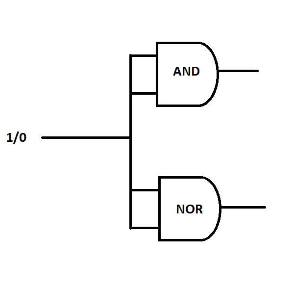
I was wondering if this (Image) can work. (Is something like this possible?)
Untitled.png

The idea is that if we have logic 1, AND gate gives 1 while NOR gives 0. And vice versa.
 

Attachments

  • Untitled.png
    Untitled.png
    2 KB · Views: 1,586
Last edited by a moderator:
Engineering news on Phys.org
  • #2
It will work.
Tying both inputs of an And/Or/Nor gate is often used for signal conditioning - or more rarely, to introduce a 1-gate delay in the signal.
 
  • Like
Likes akaliuseheal and dlgoff
  • #3
Quiz Question for @akaliuseheal -- If the input to your circuit is first a 1 and then a 0 ("1/0"), can you tell us what the output of each of the two gates will be? :smile:
 
  • #4
berkeman said:
Quiz Question for @akaliuseheal -- If the input to your circuit is first a 1 and then a 0 ("1/0"), can you tell us what the output of each of the two gates will be? :smile:
Input = 1
AND 1 | NOR 0

Input = 0
AND 0 | NOR 1
 
  • Like
Likes berkeman
  • #5
.Scott said:
It will work.
Tying both inputs of an And/Or/Nor gate is often used for signal conditioning - or more rarely, to introduce a 1-gate delay in the signal.

Thanks.
 
  • #6
Unrelated to the topic, is there any way for me to mark this thread as SOLVED since it is.
 
  • #7
The Solved checkbox is only available in the Homework Help forums, not in the technical forums. I can add it to your thread title if you like. :smile:

EDIT -- Thread title edited. :smile:
 
  • Like
Likes dlgoff and akaliuseheal
  • #8
A wise engineer once told me to be careful when configuring gate in the manner as shown above. Worth mentioning here even though it would not apply to an AND gate. In some cases of using a NAND gate as an inverter you would want to tie the input signal to just one input on the gate. Quiz question: Can anyone answer why?
 
  • Like
Likes berkeman
  • #9
Averagesupernova said:
A wise engineer once told me to be careful when configuring gate in the manner as shown above. Worth mentioning here even though it would not apply to an AND gate. In some cases of using a NAND gate as an inverter you would want to tie the input signal to just one input on the gate. Quiz question: Can anyone answer why?

I would love to know the answer to this, would it not be easier to just tie the inputs together? If you only connected one input, the other would have to go to a high, which complicates the circuit.
 
  • #10
TylerV said:
I would love to know the answer to this, would it not be easier to just tie the inputs together? If you only connected one input, the other would have to go to a high, which complicates the circuit.
Welcome to the PF. :smile:

Can you think of some reasons for only connecting the signal to one of the two inputs of the NAND gate? I can think of at least two, but I don't know if they are what @Averagesupernova was thinking of...
 
  • #11
berkeman said:
Welcome to the PF. :smile:

Can you think of some reasons for only connecting the signal to one of the two inputs of the NAND gate? I can think of at least two, but I don't know if they are what @Averagesupernova was thinking of...
I would say speed is an issue I would be worried about, and with only one input,the other input will be a constant and there would be no worry if the two values reach the gate at the same time or not
 
  • #12
I wasn't thinking along those lines... Any other thoughts? What can be typical problem issues in digital logic design?
 
  • Like
Likes sophiecentaur
  • #13
berkeman said:
I wasn't thinking along those lines... Any other thoughts? What can be typical problem issues in digital logic design?
The only other frequent problem I deal with is noise/grey area, but I don't see how that is applicable here. Tell me what you think is the problem with it?
 
  • #14
Well, the two issues I see are that when you make 2 connections to the gate, you are doubling the power required to switch the signal (for no real gain), and the increased loading on the line will reduce your fan-out for that signal by 1. That may not matter if the signal is not used anyplace else, but if you are close to the fan-out limit already for that signal, wasting one connection is not good.

@Averagesupernova may have other issues in mind... :smile:
 
Last edited:
  • #15
Sorry it took me a bit to get back here. I don't recall the exact topology of the circuit that the gate was in but it has to do with inconsistencies between individual gate inputs. Besides loading effects of more than one gate input, why use more than one input when it is not necessary? If there is a significant slew rate on the signal driving the input(s) at least with one gate there is only one input to move around and change timing over temperature range.
-
So with that said, can anyone give me a reason why gate inputs get tied together like this instead of just tying one input high when making a NOT gate out of an NAND gate? I have my ideas and in some cases it is justified to tie them together. I promise I won't leave you hanging.
 
  • #16
Averagesupernova said:
So with that said, can anyone give me a reason why gate inputs get tied together like this instead of just tying one input high when making a NOT gate out of an NAND gate? I have my ideas and in some cases it is justified to tie them together. I promise I won't leave you hanging.

I would tie them together if I was designing a pcb with many parts. This is because I do not want to have a trace going all the way to my V+ when instead I could just have the two inputs tied at the pads. At least that is my reasoning behind it, tying them would just simplify my circuit and allow me to have more space on my board for other components/traces.
 
Last edited by a moderator:
  • #17
'All the way to V+' isn't that far but it was the reason I was thinking. It is only as far as a different pin on the device. But, nonetheless it may save a designer a via or two on the PCB, etc. Often optimising which gate is used on a device can solve this.
-
I once worked for a company who's CAD system was so unreliable that whichever change to the design was least likely to crash the system is the one which was chosen.
 
Last edited:

What is a logic gate?

A logic gate is a basic building block of digital circuits. It is a physical device that performs a logical operation on one or more binary inputs and produces a single binary output. It is the fundamental component of any digital system.

What does it mean to tie both inputs of a gate together?

Tying both inputs of a gate together means connecting both input terminals of a logic gate to the same signal source. This creates a short circuit between the two inputs, so both inputs will have the same value at all times. This is known as a "direct connection" or "shorting" the inputs.

What happens when both inputs of a gate are tied together?

When both inputs of a gate are tied together, the output of the gate will always be the same as the value of the input terminals. This is because the gate's operation is based on the values of its inputs, and with both inputs tied together, they will always have the same value.

Why would someone want to tie both inputs of a gate together?

Tying both inputs of a gate together can be useful in certain scenarios, such as creating a constant logic level for a particular input. It can also be used in troubleshooting or testing circuits, as it can simplify the inputs and make it easier to analyze the behavior of the gate.

Are there any negative consequences of tying both inputs of a gate together?

Yes, tying both inputs of a gate together can have negative consequences. It can cause unexpected behavior in the circuit, or even damage the gate or other components if the signal source is too strong. It is important to carefully consider the implications before tying both inputs of a gate together.

Similar threads

  • Electrical Engineering
Replies
12
Views
1K
  • Electrical Engineering
Replies
8
Views
7K
Replies
4
Views
1K
Replies
2
Views
7K
  • Electrical Engineering
Replies
29
Views
3K
  • Electrical Engineering
Replies
9
Views
3K
  • Electrical Engineering
Replies
6
Views
2K
  • Electrical Engineering
Replies
1
Views
1K
Replies
13
Views
4K
  • Electrical Engineering
Replies
10
Views
3K
Back
Top