Fish4Fun
- 247
- 2
As a hobbyist I have had an interest in SMPS power supplies for quite some time, but have never gone past casual study of them. I understand the theory, but have difficulty with the actual implementation of things like a high-side switch mechanism for a P-Channel Mosfet.
My goal is to define a high-side switch control mechanism that will allow me to use a uController in a prototype circuit. I want to be able to use various inductors and Mosfets at different switching frequencies and duty cycles w/o designing a specific high-side switch control.
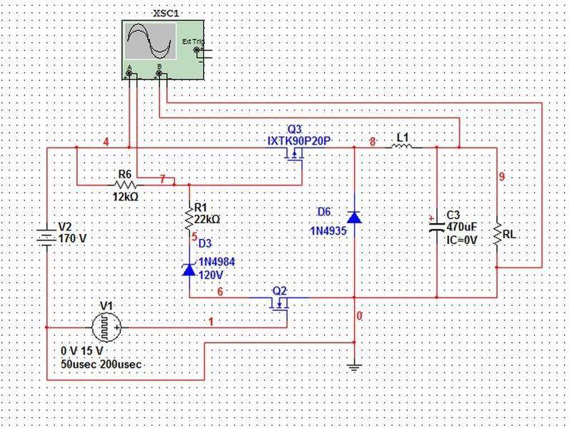
This is what I am thinking:

In simulation, it works well enough. @ 170Vdc the gate of Q3 varies between 170V and 155V. The Specs on the mosfet state that full turn-off occurs @ Vgs = -10V and Vgs can handle constant +/-20V and transient Vgs of +/-30V.
Q2 can be a fairly low voltage switch as most of the voltage is dropped by D3. The current through Q2 is fairly small, ~1.47mA. Obviously lower total resistance in the voltage divider formed by R1 & R6 will supply higher current, and thus a better switching waveform to the gate of Q3.
My question is, will the Zener/voltage divider form a viable way of switching a P-Channel mosfet? If not, is there a simple way of controlling the Gate of the P-Channel mosfet (Q3)?
Thanks in advance!
Fish
My goal is to define a high-side switch control mechanism that will allow me to use a uController in a prototype circuit. I want to be able to use various inductors and Mosfets at different switching frequencies and duty cycles w/o designing a specific high-side switch control.
This is what I am thinking:
In simulation, it works well enough. @ 170Vdc the gate of Q3 varies between 170V and 155V. The Specs on the mosfet state that full turn-off occurs @ Vgs = -10V and Vgs can handle constant +/-20V and transient Vgs of +/-30V.
Q2 can be a fairly low voltage switch as most of the voltage is dropped by D3. The current through Q2 is fairly small, ~1.47mA. Obviously lower total resistance in the voltage divider formed by R1 & R6 will supply higher current, and thus a better switching waveform to the gate of Q3.
My question is, will the Zener/voltage divider form a viable way of switching a P-Channel mosfet? If not, is there a simple way of controlling the Gate of the P-Channel mosfet (Q3)?
Thanks in advance!
Fish