Controlling an electronic load across two ground domains

In summary: Yes, you would make a miller integrator by connecting the (-) input of U3 to the junction of R2 and C1.
  • #1
gnurf
370
8
Please refer to the simplified circuit in the attached figure. The overall goal is to control the current through sense resistor R1 by adjusting a reference voltage V2, thus creating an electronic load where the power is dissipated in Q1. All load current is returned locally in the isolated loop on the right. By sensing the current differentially with e.g. AD629 and using the output as an error signal, U3 should to my mind simply drive Q1 to whatever level necessary thus closing the loop. However, in weak moments I start to think about what exactly is the relationship between the gate and source of Q1 since they are referenced to different ground domains. Is something off here?
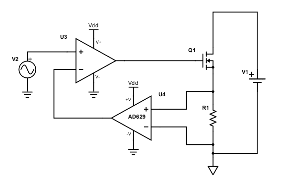
Floating_load.png
 

Attachments

  • Floating_load.png
    Floating_load.png
    4 KB · Views: 368
Engineering news on Phys.org
  • #2
You have not specified how the grounds are related.

There is a real problem with that circuit. I would expect an analogue isolator between the op-amp output and the gate input voltage.

As the design is now, the op-amp output will have to track the control signal plus the differential ground noise.
There is no low-pass filter in the feedback loop, so it will probably behave like a switching PWM controller. The error amplifier needs to become an integrator before it drives the isolator.
 
  • Like
Likes berkeman and anorlunda
  • #3
For the sake of the argument the grounds are isolated from each other. In fact, I could've removed the "analog ground" symbol and pretended the right loop was a battery. I have simulated this whole thing with correct models etc and concluded, if only temporarily, that the circuit worked after I tamed the inevitable oscillations with a RC series pair across U3's negative input to output. Does that count as your integrator? The controlling ref voltage V2 is in reality a DC value that changes only slowly e.g. when the user adjusts the current set level.

Please see the updated figure below (it's still simplified--I'll shed more light as necessary).

Floating_load_v2.png
 
  • #4
Baluncore said:
I would expect an analogue isolator between the op-amp output and the gate input voltage. [...] As the design is now, the op-amp output will have to track the control signal plus the differential ground noise. [...]
Galvanic isolation is not a requirement per se--it just so happens that the loop on the right is not referenced to the same ground as the left loop. Why is an isolator necessary?

Can you help me understand why the output will track the differential ground noise? To my mind, U3 will simply drive the gate such that its two inputs are equal, the effect of which propagates back through U4, ultimately forcing a portion of the set voltage across R1.
 
  • #5
gnurf said:
For the sake of the argument the grounds are isolated from each other.
Then you have defined the two wire "circuit" as having only a single connection. It cannot work because there is no current available to charge the gate capacitance.

If the grounds really are floating then why can you not simply join them at one point?

The MOSFET Q1 will have zener-diode protection of the gate-source voltage to prevent electrostatic destruction of the gate. That is one connection between the different grounds. The other is the input resistance of the instrumentation amplifier, U4.

Your series R2, C1 is not an integrator. Move the (-)input of the error-amplifier U3, to the junction of R2 with C1, which will make a miller integrator.

But you are still missing an isolator, or a ground cross-connection.
Until you relate those two grounds your circuit will remain a mess of confusion.

An isolator will require a power supply on the MOSFET side. What is the V1 supply voltage specification?
 
  • #6
gnurf said:
Please see the updated figure below (it's still simplified--I'll shed more light as necessary).
It is necessary now. You do not appear to know what you are doing, so you are in no position to decide what is going to be relevant.

gnurf said:
In fact, I could've removed the "analog ground" symbol and pretended the right loop was a battery. I have simulated this whole thing with correct models etc and concluded, if only temporarily, that the circuit worked ...
Go ahead and do that. Also inject a sinewave or random +/- 50 volt signal between the two separate grounds and see how it responds. Then you will appreciate the monster you have created.

What have you used to model the circuit?
 
  • #7
gnurf said:
Galvanic isolation is not a requirement per se--it just so happens that the loop on the right is not referenced to the same ground as the left loop. Why is an isolator necessary?
It is needed because the loop on the right is not referenced to the same ground as the left loop.
 
  • #8
Thanks for your patience--your frustration re my attempt to trickle down information is probably warranted. Unfortunately I don't own the schematic so I can't post it here.

In an attempt to recreate the important parts of the circuit from memory I omitted the output resistor of U4, which I believe will complete the Miller integrator you describe. R2 still seems to be necessary though if my spice simulation is anything to go by--it is critical to my ability to dampen the oscillations I observed in simulation.

The difference ampflier AD629 has about 400k from Vin(-) to Vout. Doesn't that provide the return path for the charging of Cgs? Is an isolator still required despite this?

In the actual circuit the two ground domains will probably be connected at some point. However, that connection is out of my control so I just wanted to see if I could design as if it wasn't there.

In summary, given the completed Miller integrator, return path through AD629, and the the somewhat loosely defined (probably off-board) ground relationship, do you still think this is going to end bad?
 
  • #9
gnurf said:
The overall goal is to control the current through sense resistor R1 by adjusting a reference voltage V2, thus creating an electronic load where the power is dissipated in Q1.
So you want to be able to set the load current, not the load power, right? Can you say a bit more about the application? In my experience, it is more common to want a constant power load rather than a constant current load.

Also, what voltage range is V1? Is it below SELV? If not, that may be a reason that you need galvanic isolation between the right-side circuit and the low-voltage control circuit on the left. What is the power source for the control circuitry on the left? Is it a double-insulated power supply with no user access to any of the control circuitry? What safety certifications are you planning for this device?

I'm assuming that the voltage source V1 is DC? If it is variable (but still unipolar), how quickly can it change?

EDIT/ADD -- Also, what sort of enclosure are you planning for this? An Earth Grounded metal enclosure? A plastic enclosure (with a double-insulated power supply)?
 
Last edited:
  • #10
gnurf said:
For the sake of the argument the grounds are isolated from each other. In fact, I could've removed the "analog ground" symbol and pretended the right loop was a battery. I have simulated this whole thing with correct models etc and concluded, if only temporarily, that the circuit worked after I tamed the inevitable oscillations with a RC series pair across U3's negative input to output. Does that count as your integrator? The controlling ref voltage V2 is in reality a DC value that changes only slowly e.g. when the user adjusts the current set level.

Please see the updated figure below (it's still simplified--I'll shed more light as necessary).

View attachment 247060

I've built a few little loads here and there using basically the same circuit.

As others have mentioned as drawn this won't work, the grounds for the current and error amplifier should be the same ground as the load elements.

The AD629 is a crazy amplifier with +/-270V common mode capability! I assume you chose this part because of the isolation?

I'd do this a little differently:

Putting the isolation barrier inside your control loop makes things needlessly problematic from a stability point of view, so I'd put the opamps on the same ground as the load, and use an isolator (eg opto or what ever) to relay your setpoint signal over the isolation barrier (assuming you must have this isolation). This way you can use normal opamps, something that can go to 15V supply, (a little dual opamp something like LM2904Q1). One to do the current sense amplification, the other to do your error amplifier, strictly speaking of you want to do "true" PI control (assuming you want your steady state error to be zero, you need to integrate) you need to do the K and I separately:
1563992032224.png
U1 is error amp, U2 integrates, U3 is the proportional gain, U4 is the summation amplifier to bring it all back together.

Depending on how picky you are something like below can often be enough:

1563992056700.png


I'd also add a small resistive element between the drain and the load input, this makes the power dissipation on the fet(s) a little easier to manage, and reduces the overall gate voltage to current gain, this makes it a little easier to stabilize the whole thing.

Also for me at least, one fet was never enough, its always been at least a kw or so load, so needed quite a few parallel devices, which brings in a whole host of other things to keep in mind, (like source degeneration resistors).
 
  • Like
Likes berkeman
  • #12
As others have said, you'll need to ground the negative side of the battery.
You'll also want to add a resistor in series with the output of the current sense amp to make your integrator work properly. In fact, you could do this with a single op-amp if you wanted. Look up "differential integrator" if your interested.
Since you haven't included any numbers we can't tell if you are dealing with mW of KW, so we can only give general advice.
If the voltage across R1 is small compared to Vgs, then this circuit should work fine. In fact, this is a very common circuit for what you are trying to do.
The source resistor will tend to stabilize the circuit with local negative feedback. You can look up "source follower" (or "emitter follower" for BJTs) to learn more about this.
Your amplifier will have to accept signals at ground potential, of course.
You still have a bunch of details to work out, but there is nothing fundamentally wrong with your plan.
 
  • #13
berkeman said:
So you want to be able to set the load current, not the load power, right? Can you say a bit more about the application? In my experience, it is more common to want a constant power load rather than a constant current load.

Also, what voltage range is V1? Is it below SELV? If not, that may be a reason that you need galvanic isolation between the right-side circuit and the low-voltage control circuit on the left. What is the power source for the control circuitry on the left? Is it a double-insulated power supply with no user access to any of the control circuitry? What safety certifications are you planning for this device?

I'm assuming that the voltage source V1 is DC? If it is variable (but still unipolar), how quickly can it change?

EDIT/ADD -- Also, what sort of enclosure are you planning for this? An Earth Grounded metal enclosure? A plastic enclosure (with a double-insulated power supply)?

Thanks, Berkeman. V1 is a fixed and known voltage below 60V (=SELV?) so the load power can be calculated if needed. The power source on the left will be a commerical AC/DC adapter, wall-wart type of thing. It's not a commercial product so no certification or even enclosure is planned.
 
  • Like
Likes berkeman
  • #14
essenmein said:
[...] The AD629 is a crazy amplifier with +/-270V common mode capability! I assume you chose this part because of the isolation?

I'd do this a little differently:

Putting the isolation barrier inside your control loop makes things needlessly problematic from a stability point of view, so I'd put the opamps on the same ground as the load, and use an isolator (eg opto or what ever) to relay your setpoint signal over the isolation barrier (assuming you must have this isolation).

[...]

Also for me at least, one fet was never enough, its always been at least a kw or so load, so needed quite a few parallel devices, which brings in a whole host of other things to keep in mind, (like source degeneration resistors).
Thanks for that detailed reply, I'll have to review it more closely at a later time.

Actually, my first draft of this circuit did in fact have the control loop on the load side, but for various reasons I drifted away from that idea and, perhaps, lost my ways in the process. This project has been a bit on and off so my memory might be failing me now, but I think one of the issues that stymied back then was how to accurately relay the setpoint DC value across an isolation barrier. Thinking about it now, my initial reaction is that they probably do this all the time (successfully) in e.g. isolated power supplies and that I might have spooked myself with some nonsense and forked off in the wrong direction. I should probably look into that again, if nothing else to clear out some misconceptions on my part. Do you have any concrete leads on that topic? Are we talking jellybean parts here?

Anyway, the AD629 seemed like a good fit with its differential input, CM capability and bias options, the latter being necessary as it bottoms out at a bit over 1V somewhere.

This load is only up to 60W so finding a FET that I can operate in the SOA is trivial compared to the load levels you mention.

EDIT: Fixed typo.
 
  • #15
DaveE said:
As others have said, you'll need to ground the negative side of the battery.
You'll also want to add a resistor in series with the output of the current sense amp to make your integrator work properly. In fact, you could do this with a single op-amp if you wanted. Look up "differential integrator" if your interested.
Since you haven't included any numbers we can't tell if you are dealing with mW of KW, so we can only give general advice.
If the voltage across R1 is small compared to Vgs, then this circuit should work fine. In fact, this is a very common circuit for what you are trying to do.
The source resistor will tend to stabilize the circuit with local negative feedback. You can look up "source follower" (or "emitter follower" for BJTs) to learn more about this.
Your amplifier will have to accept signals at ground potential, of course.
You still have a bunch of details to work out, but there is nothing fundamentally wrong with your plan.
Thanks for the "differential integrator" pointer, I'll check that out. For this project, however, I kind of liked the robust AD629 as the interface to the load side (which is out of my control and thus assumed abusive). The AD629 is in fact followed by a level shifter/amplifier (not shown in the figures) which puts the control signal back into the range of the reference (set) voltage. As I said elsewhere, I have simulated this in its entirety and thought I had the details down--but apparently the spice model fails to take into account that the mosfet is doing a split between different ground domains. That doesn't align with my previous experience with spice, but who trusts simulators anyway.

The sense resistor is 0.1 Ohm and the current range is 0 to 1A so the voltage across it will be negligible compared to Vgs.
 
  • #16
gnurf said:
The difference ampflier AD629 has about 400k from Vin(-) to Vout.
Correction: I was about to change this from Vout to GND because I thought it was a typo, but it's actually 400kOhm from Vin(-) to a reference voltage pin I see now. So it's 400k plus whatever the Vref resistance to GND is. I guess "isolated" and "400k++" is pretty much the same thing here, so the point is probably moot anyway.
 
Last edited:
  • #17
This misbegotten project has so many problems that they are colliding with each other. There is insufficient information to give sensible advice. Any changes suggested just confuse things more.

For example; If R1 is the output load, then Q1 is an N-channel source-follower, and will need a gate voltage that swings from zero to V1 plus a few volts. Even with a ground connection, I doubt U3 will have the required output voltage swing of 60+ volts.

What really is the load R1? Is this a DC motor speed controller?
What current and voltage can appear across R1 ?
 
  • #18
gnurf said:
I think one of the issues that stymied back then was how to accurately relay the setpoint DC value across an isolation barrier.
For a 0-10V lighting controller output voltage, we use a PWM signal from our control processor to cross the opto barrier. The PWM percentage is controlled pretty well (to less than 1%), and the analog circuit on the other side of the optos averages the PWM as its input, and monitors the output voltage to ensure that it is the correct percentage of the maximum 10V output.

There are other precision ways to transmit analog values across an opto barrier, but PWM is a pretty good one in some applications.
 
  • Like
Likes Averagesupernova
  • #20
Baluncore said:
For example; If R1 is the output load, then Q1 is an N-channel source-follower, and will need a gate voltage that swings from zero to V1 plus a few volts. Even with a ground connection, I doubt U3 will have the required output voltage swing of 60+ volts.

What really is the load R1? Is this a DC motor speed controller?
What current and voltage can appear across R1 ?
R1 is not the load, it's a 0.1 Ohm sense resistor. The load is Q1 which is operated in its current saturation region.

It seems I have two choices going forward:

1) connect the grounds, in which case I can among other things also get rid of AD629 to simplify the circuit.
2) find a way to isolate the gate drive signal.

Do you agree?
 
  • #21
berkeman said:
For a 0-10V lighting controller output voltage, we use a PWM signal from our control processor to cross the opto barrier. The PWM percentage is controlled pretty well (to less than 1%), and the analog circuit on the other side of the optos averages the PWM as its input, and monitors the output voltage to ensure that it is the correct percentage of the maximum 10V output.

There are other precision ways to transmit analog values across an opto barrier, but PWM is a pretty good one in some applications.
Thanks. My first crack at this was in fact a PWM based design which made the isolation barrier problem easy as described in your post here. I had a spare opamp so I used a small Sallen-Key filter to average the output on the load side before using that as a control signal. All the analog stuff was on the load side, powered by local regulators that fed of the 60V rail. So the grounding scheme was pretty much in line with what essenmein described in post #10, I believe (having only skimmed through his schematics).

EDIT: The reason the PWM approach was scrapped, I might add, is another story that involves humans.
 
  • Like
Likes berkeman
  • #23
gnurf said:
R1 is not the load, it's a 0.1 Ohm sense resistor. The load is Q1 which is operated in its current saturation region.
So what you have is a heater with a MOSFET as the element. As R1 is an 0.1 ohm sense resistor, the last thing you need to do is divide that small voltage by 20, which is exactly what the AD629 does.

gnurf said:
It seems I have two choices going forward:
1) connect the grounds, in which case I can among other things also get rid of AD629 to simplify the circuit.
2) find a way to isolate the gate drive signal.
Do you agree?
No. I am sorry about being brutally honest when I say that there are many problems with this design. One change will not fix it.
Another example: Notice that the AD629 output cannot approach within 2 volts of the negative supply, or 1.5 volt of the positive supply. If the AD629 is used then the supply needs to be more sophisticated, so the lower terminal of R4, the pot voltage is the same as the zero reference on the AD629, which must be 2V or more above Vneg supply, = ground in your diagram.

If the problem was specified it could be solved reliably, and with a few components. But there is no specification. We do not know the output current, nor what the load really is, or why.

Why do you not derive the Vdd power supply from the V1 = 60V rail ?
 
  • #24
Baluncore said:
So what you have is a heater with a MOSFET as the element. As R1 is an 0.1 ohm sense resistor, the last thing you need to do is divide that small voltage by 20, which is exactly what the AD629 does.
Yes, it's a heater aka an electronic load. The AD629 does indeed attenuate by 20 as you say, but the gain is also internally restored and the transfer function is ultimately Vout = V(+IN) - V(-IN), ref page 10 in the datasheet.
Baluncore said:
No. I am sorry about being brutally honest when I say that there are many problems with this design. One change will not fix it.
Don't be sorry, I'm thankful for all feedback.
Baluncore said:
Another example: Notice that the AD629 output cannot approach within 2 volts of the negative supply, or 1.5 volt of the positive supply. If the AD629 is used then the supply needs to be more sophisticated, so the lower terminal of R4, the pot voltage is the same as the zero reference on the AD629, which must be 2V or more above Vneg supply, = ground in your diagram.
I add a DC bias (+4.096V) to the AD629 output in order to avoid your concern here about the lack of room near the negative rail (GND). I then amplify and strip off the bias downstream and feed the result (0V to 4.096V, which now corresponds to 0A to 1A load current) to the "error amplifier" where it is compared to the output from a DAC (also 0V to 4.096V).
Baluncore said:
If the problem was specified it could be solved reliably, and with a few components. But there is no specification. We do not know the output current, nor what the load really is, or why.

Why do you not derive the Vdd power supply from the V1 = 60V rail ?
The output current is 0 to 1A. The load is Q1 and it's because it is an electronic load. I just need to draw a programmable amount of current from a device under test. V1 will be nominally turned off and activated by another system, so I can't rely on that (this is just a small subsection of a larger board which has other duties as well).

If I can get the optocoupler model working, I'll see if I can make a complete model of what I'm trying to do (i.e. option 2 from post #20) and add it here. I probably should've done that straight away, given the wall of text that is unfolding here. Thanks.
 
  • #25
gnurf said:
Thanks for that detailed reply, I'll have to review it more closely at a later time.

Actually, my first draft of this circuit did in fact have the control loop on the load side, but for various reasons I drifted away from that idea and, perhaps, lost my ways in the process. This project has been a bit on and off so my memory might be failing me now, but I think one of the issues that stymied back then was how to accurately relay the setpoint DC value across an isolation barrier. Thinking about it now, my initial reaction is that they probably do this all the time (successfully) in e.g. isolated power supplies and that I might have spooked myself with some nonsense and forked off in the wrong direction. I should probably look into that again, if nothing else to clear out some misconceptions on my part. Do you have any concrete leads on that topic? Are we talking jellybean parts here?

Anyway, the AD629 seemed like a good fit with its differential input, CM capability and bias options, the latter being necessary as it bottoms out at a bit over 1V somewhere.

This load is only up to 60W so finding a FET that I can operate in the SOA is trivial compared to the load levels you mention.

EDIT: Fixed typo.

As someone else mentioned PWM is a good way to get around the isolation linearity issue, analog has some fancy "isolation amplifiers" (eg AD215) if you wanted to remain analog. However if this is just a lab thing, and you're only dealing with a few volts or so, I'd probably just handle the isolation aspect with a plastic knob on the pot. Unless the pot is just a representation of a variable command voltage coming from another part (eg MCU), and if its coming from a micro, just get the software guy to put out a PWM signal directly that you can then send easily over the iso barrier and low pass filt for the set point current.
 
  • #26
essenmein said:
As someone else mentioned PWM is a good way to get around the isolation linearity issue, analog has some fancy "isolation amplifiers" (eg AD215) if you wanted to remain analog. However if this is just a lab thing, and you're only dealing with a few volts or so, I'd probably just handle the isolation aspect with a plastic knob on the pot. Unless the pot is just a representation of a variable command voltage coming from another part (eg MCU), and if its coming from a micro, just get the software guy to put out a PWM signal directly that you can then send easily over the iso barrier and low pass filt for the set point current.
Yeah, the control is from a MCU, but it's a DAC output and not a PWM. I've been down the latter path already (and probably should've stayed on it as well), see post #21.
 
  • #27
OK, so I hacked together something which seems to do what I want which is to control the load current by adjusting the output of a DAC. What is new here, well to me anyway, is the IL300 optocoupler suggested by @Tom.G in post #19 which I think solves the issue with floating grounds mentioned by @Baluncore and others. I'm a bit hesitant to post the whole .asc file, but if someone wants to have a look (or just wants it for whatever reason--I don't care) I can send it off-thread.

If there are any fundamental issues here (still) I'd be glad if someone could point them out. E.g. I'm sure I've butchered the so-called Miller integrator; the values are chosen by trial and error but it seems to work. I can easily break the whole thing by reducing for example R6 to say 20K or less. Also, I get that the optocoupler probably lives a happier life outside of the control loop, but for something as crude as this it hopefully can be acceptable.

Note: The 1MEG resistors in the schematic were added due to convergence issues and can be disregarded.

isoload_v1.png

The plot below shows how the load current tracks the DAC input to U1. If someone can think of another test that actually breaks this, then that would be great.

isoload_plot_v1.png


Datasheets:
 
  • #28
Not necessarily problems, just a couple concerns.

1) It is unclear if the +VREF for U2 and U3 are separately derived as they need to be. The VREFs for U3 must be generated on the GND_iso portion of the circuit, while the VREF for U2 must be generated on the other, non-GND_iso, side.
SEE MY POST #30 BELOW

2) Please check the loop gain of the overall circuit, especially the gain distribution among the stages. If I did the quicky estimate correctly I get a transconductance of 79 A/V from the DAC voltage input, that seems quite high for your stated current range.

Cheers,
Tom
 
Last edited:
  • #29
The circuit has grown in complexity again, and again.
I no longer believe anything I read in this thread.

How would I do it?
I would have kept the control voltage DAC on one side as a two terminal voltage source that changes from zero to 4.096 V. That requires only two thin tracks cross the ground discontinuity. Keep it simple.

Everything else would be powered and referenced to the load side supply. The AD629 would be powered from the load side and would sense the DAC differential output voltage only. There is then no requirement for any opto-isolator loop of any sort. The control loop becomes trivial as it compares two voltages.

A 100k resistor across the AD629 inputs will zero the load current when the DAC is not powered.
Loss of load side power will not load the DAC because the AD629 input resistance is high voltage.
 
  • #30
Ignore part 1) of my post #28 above r.e. the REF voltages.

A more thorough reading of the AD629 datasheet reveals that the Output is referenced to the REF pins 1&5. The datasheet also shows that the maximum isolation resistance from Input or REF to Output to be 400k. And the maximum CM voltage for your configuration is about 125V.

The consequences of this are that most of the circuitry should be on the GND_iso side and the DAC voltage should be fed in thru optical isolation. This would also allow replacing the AD629 with a lower cost device if desired.

A minor circuit 'convenience change' could be to use a Rail Splitter virtual ground to shift the op-amp reference to 1/2 the supply voltage.
See for example: http://www.ti.com/product/TLE2426

Cheers,
Tom

(p.s. I think we're getting there)
 
  • #31
Here is a proof of concept. LTspice .asc attached as floatearth.asc.txt, remove .txt to run it.
DAC produces Vdac, perched on 50 volts of AC noise.

Pre-regulator makes Vpr ≈ 12 volt rail. Select a cheaper MOSFET, adjust zener voltage.
No model here for a 5 volt regulator following Vpr, here it is V7805. Called Vcc = 5V.
Supply rails do not need to be precise.

I have no model for the AD629 chip. Replace B_AD629 with a model.
Select two op-amps for Rail to Rail input and 15V supply.

schematic.png


waveform.png
 

Attachments

  • floatearth.asc.txt
    4.1 KB · Views: 131
  • #32
Baluncore said:
DAC produces Vdac, perched on 50 volts of AC noise.
Not having used DACs for decades, I have a couple questions.
Are DACs available with 50V isolation between the digital input and analog output?
If the DAC is voltage output, what is the source for the Reference input?
 
  • #33
Tom.G said:
Are DACs available with 50V isolation between the digital input and analog output?
Not DtoA that I know of. There are isolated AtoD available. Isolation of serial data input is most energy economic, so if isolated DtoA were available it would probably be with a serial data I/F.
https://www.analog.com/en/products/interface-isolation/isolation.html
Tom.G said:
If the DAC is voltage output, what is the source for the Reference input?
I believe most voltage output DACs now have an inbuilt reference voltage that can be selected.
Early DACs had an external current or voltage reference.
 
  • #34
gnurf said:
OK, so I hacked together something which seems to do what I want which is to control the load current by adjusting the output of a DAC. What is new here, well to me anyway, is the IL300 optocoupler suggested by @Tom.G in post #19 which I think solves the issue with floating grounds mentioned by @Baluncore and others. I'm a bit hesitant to post the whole .asc file, but if someone wants to have a look (or just wants it for whatever reason--I don't care) I can send it off-thread.

If there are any fundamental issues here (still) I'd be glad if someone could point them out. E.g. I'm sure I've butchered the so-called Miller integrator; the values are chosen by trial and error but it seems to work. I can easily break the whole thing by reducing for example R6 to say 20K or less. Also, I get that the optocoupler probably lives a happier life outside of the control loop, but for something as crude as this it hopefully can be acceptable.

Basically if using an opto as a linear device its best to wrap a control loop around it since they are not very good at being linear, you'd have to use PWM or something if the opto was open loop.

Beyond me doing an actual schematic review, on the surface what you have should work.

Regarding the whole current sense thing, I don't know if I like using high CM input amplifier to achieve this isolation thing, which is hilarious because that's precisely what I'm using (INA series from ti) although its sensing phase current in poly phase inverter (so the CM amplifier rejects the PWM voltage), so grounds are ~ same, well they beep out with multi meter, but due to the 100's of A of current being switched very quickly, there is a lot of inductive kick generating ~10V transients at full load. The seem to do the job well and haven't failed yet after some pretty nasty life testing, so maybe my "feelings" are off here.

Have you considered something like hall based contactless sensing? Would certainly put to bed any concerns re different grounds on the sense amplifier.

Eg:
https://www.melexis.com/en/products/sense/current-sensorshttps://www.allegromicro.com/en/Pro...-To-Fifty-Amp-Integrated-Conductor-Sensor-ICs
 
  • #35
@Baluncore I asked about the 50V isolation
Tom.G said:
Are DACs available with 50V isolation between the digital input and analog output?

Baluncore said:
Not DtoA that I know of. There are isolated AtoD available. Isolation of serial data input is most energy economic, so if isolated DtoA were available it would probably be with a serial data I/F.

because the schematic you show has the digital ground on one circuit and the analog output connected to a device with Gnd reference different by 50V . I was wondering if this is an appropriate configuration.
https://www.physicsforums.com/attachments/schematic-png.247128/
And the question about the DAC reference source has the same concern. The internal switching transistors in the DAC will be subject to the 50V Gnd difference if they are driven directly by the digital logic.

In light of the above, I believe the DAC must have galvanic isolation to avoid the different Gnd voltages appearing between the digital and analog pins.

Cheers,
Tom
 

Similar threads

  • Electrical Engineering
Replies
12
Views
2K
  • Electrical Engineering
4
Replies
138
Views
22K
  • Electrical Engineering
Replies
4
Views
3K
  • Electrical Engineering
Replies
19
Views
2K
  • Electrical Engineering
Replies
1
Views
5K
  • Engineering and Comp Sci Homework Help
Replies
1
Views
3K
  • Introductory Physics Homework Help
Replies
1
Views
1K
  • Beyond the Standard Models
Replies
18
Views
3K
  • High Energy, Nuclear, Particle Physics
Replies
19
Views
3K
Back
Top