Discussion Overview
The discussion revolves around how to create an inverter using a two-input NAND gate. Participants explore the connections and configurations necessary to achieve the desired functionality, focusing on the theoretical and practical aspects of digital logic design.
Discussion Character
- Exploratory, Technical explanation, Conceptual clarification
Main Points Raised
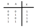
- One participant inquires about the connection of a two-input NAND gate to form a basic inverter and mentions constructing a truth table, noting that only certain input combinations are relevant.
- Another participant points out that a basic inverter typically has only one input and asks for ways to adapt a two-input device to function as a one-input device.
- A participant seeks clarification on whether both inputs of the NAND gate need to be the same to produce a single output value for the inverter.
- One participant suggests experimenting with tying the two inputs of the NAND gate together and encourages others to analyze the resulting truth table to determine if it meets the inverter's requirements.
Areas of Agreement / Disagreement
Participants do not reach a consensus on the best method to create an inverter from a NAND gate, and multiple approaches and interpretations are presented without resolution.
Contextual Notes
Some assumptions about the behavior of NAND gates and the requirements for an inverter are not explicitly stated, and the discussion does not resolve the implications of tying inputs together.
Who May Find This Useful
Individuals interested in digital logic design, electronics, or those studying basic circuit theory may find this discussion relevant.