Hysteresis of a voltage comparator

In summary: LED. The comparator is being powered by a 12V voltage source and the resistors used are not known. The ideal hysteresis voltage is a little bit more than the peak-to-peak noise content of the Vin signal, and for a production circuit in a quiet environment, it is recommended to use three to five times the standard deviation of the noise. The purpose of R3 in the circuit is to pull the output pin to a high state, and it is necessary to calculate its value based on the desired output voltage. The LM393 comparator is being used and it is important to choose resistors that
  • #1
akaliuseheal
53
8
Hello,
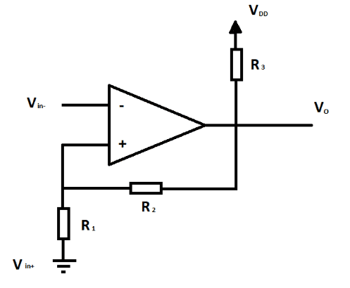
I am designing a circuit which basically takes two voltages (V1,V2) and based upon which one of the two is greater, turns corresponding LED. So, I have got to the part where I have output from differential op amp that is the input of the inverting voltage comparator with hysteresis. Comparator compares that voltage with ground, which tells me whether that voltage is positive or negative or V1>V2 , V1<V2 . Comparator is shown bellow.
123.PNG

Minimal input voltage is ±0.72V, voltage used to power the comparator is 12V, resistors are not known.

Questions:

  1. What is the ideal hysteresis voltage, a little less than minimal input voltage?
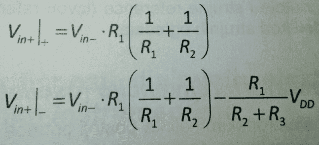
  2. I have found some expressions in the book and if someone is willing to clarify them( which value is which apart from the resistors ) it would help.
It says:
Output voltage will change based upon voltages given by these expressions.
456.PNG
 

Attachments

  • 123.PNG
    123.PNG
    3.1 KB · Views: 2,762
  • 456.PNG
    456.PNG
    44.3 KB · Views: 1,200
Engineering news on Phys.org
  • #2
It takes very little hysteresis to switch cleanly. 5 mV was built into many comparators in the good old days.
The hysteresis should be greater than (Output voltage swing) / (open loop gain).

A voltage comparator can operate with a big differential input voltage. But an Op-amp is designed to operate in a closed loop with very low differential input voltage. You will need to check that your selected op-amp behaves well as a comparator.
 
  • Like
Likes akaliuseheal and Tom.G
  • #3
akaliuseheal said:
What is the ideal hysteresis voltage, ...?

I'd say a little bit more than the peak-to-peak noise content of your Vin signal.
 
  • Like
Likes sophiecentaur and akaliuseheal
  • #4
jim hardy said:
I'd say a little bit more than the peak-to-peak noise content of your Vin signal.
For experimenting that's fine, and you can always increase it if needed.

For a production circuit in a moderately quiet environment, I would say three to five times the standard deviation of the noise to handle its random nature. In a noisy environment, three to five times the highest peak noise you have observed (and add some filtering).
 
  • Like
Likes akaliuseheal
  • #5
We need more information about the noise profile of your signal.
Also, what do you mean, or how do you define “minimal input voltage” = ±0.72V.

When the comparator switches between low and high output voltages, that voltage swing appears at the non-inverting input, attenuated by the R1 + R2 potential divider.
 
  • #6
Baluncore said:
We need more information about the noise profile of your signal.
Also, what do you mean, or how do you define “minimal input voltage” = ±0.72V.
Input comes from differential op amp which takes two fixed values of voltage(14 total fixed values that originate from representation of resistance as voltage in the first step of the device). ±0.72V being the closest to 0.
About the noise, this won't be commercial product and I'm a beginner in this. I have no information about noise.

Baluncore said:
When the comparator switches between low and high output voltages, that voltage swing appears at the non-inverting input, attenuated by the R1 + R2 potential divider.

But, what is the purpose of R3?
 
  • #7
akaliuseheal said:
But, what is the purpose of R3?
R3 is called a "Pull Up Resistor".
Its purpose is to "pull" the output pin to a high state.
That let's you use the comparator to drive logic level circuits where the maximum permissible voltage might be 5 or 3.3 volts not the 12 used by your analog circuitry.

Many comparators are built with no internal output current (high) drive for their output pin, they can only sink current to pull the pin low.
That's on purpose so you can use them to interface between analog and logic circuits that use different supply voltages , and to let you connect several outputs in parallel for "wired or" logic.
It's called "Open Collector" or "Open Drain" .
here's the inside of a TI LM139 comparator , from http://www.ti.com/lit/ds/symlink/lm239a.pdf

upload_2018-9-11_4-33-25.png


So, to your question - R3 provides current to drive the output to its high voltage state, ie "Pull it up" .

What comparator are you using ?

old jim
 

Attachments

  • upload_2018-9-11_4-33-25.png
    upload_2018-9-11_4-33-25.png
    25.7 KB · Views: 1,080
  • #8
here's a tutorial on comparators
https://www.electronics-tutorials.ws/opamp/op-amp-comparator.html
 
  • #9
jim hardy said:
here's a tutorial on comparators
https://www.electronics-tutorials.ws/opamp/op-amp-comparator.html

Okay, so, if I were to use lm393 and if I wanted UTP = 0.6, LTP = -0.6

±(R1 / R1 + R2 ) * V
±( 56 / 56 + 1000 ) * 12 ≈ 0.6
R1 = 56Ω
R1 = 1000Ω

How would I calculate R3?
I don't really know how to read datasheet and on the output I need voltage of 5V.
 
  • #10
akaliuseheal said:
How would I calculate R3?
I don't really know how to read datasheet and on the output I need voltage of 5V.
Recalculate R1 and R2 using Vout of 5 volts
Then calculate R3 to make a voltage divider with your new R1 & R2 to give 5 volts at Vout.


old jim
 
  • #11
jim hardy said:
Recalculate R1 and R2 using Vout of 5 volts

100 / ( 100+140 ) * 12 = 5
R1 = 100Ω, R2 = 140Ω

jim hardy said:
Then calculate R3 to make a voltage divider with your new R1 & R2 to give 5 volts at Vout.

How do you mean?
 
  • #12
akaliuseheal said:
How do you mean?

5 volts across (100 + 140 )ohms = 5 / 240 = 0.02083 amp,
and when output is 5 volts that current must all flow down through R3 because the open drain can't source current It can only sink ..
So,
What value of R3 would drop the remaining 7 volts between your Vo pin and your 12 volt VDD source ?

R = E/I = 7 / 0.02083 = 336 ohms

That of course neglects any current required by whatever the Vo pin drives.
And one should check the datasheet to make sure the device is rated to sink those 20.83 milliamps.
 
  • Like
Likes akaliuseheal
  • #13
LM393 datasheet says, in line "Output Sink Current" the chip will sink at least 6 milliamps and typically 16 milliamps.
So good design using that comparator would suggest use of higher values for R1 R2 and R3.

Can you find three resistors that give your desired trip and reset points yet only require the IC to sink 6 ma ?

That would be a good design.
 
  • Like
Likes Tom.G
  • #14
jim hardy said:
Can you find three resistors that give your desired trip and reset points yet only require the IC to sink 6 ma ?

That would be a good design.

Well, R1 = 342 and R2 = 480
Gives:
I = 5 / ( 342 + 480 ) = 0.006 amps
R = 7 / 0.006 = 1167 ohms
 
  • Like
Likes jim hardy
  • #15
You're catching on quick !

Study the application hints in datasheets
and become familiar with device ratings.
 
  • Like
Likes akaliuseheal
  • #16
jim hardy said:
You're catching on quick !

Study the application hints in datasheets
and become familiar with device ratings.

Huge thanks to you, thank you for your time.

Edited
 
  • Like
Likes jim hardy
  • #17
I hope you build one and it works great...
Good luck in your studies..

old jim
 
  • Like
Likes dlgoff and akaliuseheal
  • #18
jim hardy said:
I hope you build one and it works great...
Good luck in your studies..

old jim

Sorry to bother you, I was away for 3 days and I wanted to look over this thread again and I have also seen that you answered on that "reading datasheet" thread so thank you for that also.
Now, going thru it again, what confuses me is when we recalculated values of R1 and R2. Are those the new values of R1 and R2 and if not, why was that step necessary.

To sum it up:
R1 = 56 Ω
R2 = 1000 Ω
R3 = 1167 Ω
or
R1 = 342 Ω
R2 = 480 Ω
R3 = 1167 Ω
 
  • #19
i was away too , will have to get back up to speed. I don't think i checked your calculations - would you show them ?
 
  • #20
jim hardy said:
i was away too , will have to get back up to speed. I don't think i checked your calculations - would you show them ?
I figured out the correct values but I still don't see the point in this:
Recalculate R1 and R2 using Vout of 5 volts
Then calculate R3 to make a voltage divider with your new R1 & R2 to give 5 volts at Vout.

That was to calculate resistance of a pull up resistor so that logic 1 has value of 5V.
Why that step? When R = V / sink_current, where V = Vdd - voltage_wanted_on_the_output
 
  • #21
akaliuseheal said:
but I still don't see the point in this:
That was to calculate resistance of a pull up resistor so that logic 1 has value of 5V.
Why that step? When R = V / sink_current, where V = Vdd - voltage_wanted_on_the_output

Look back at post #1 where you were uncertain about those equations from your book.

I just wanted you to start from scratch and figure out how to calculate the resistors , independently.

I hadn't checked those formulas myself so didn't trust them.
As you point out it's not a difficult calculation.

old jim
 

1. What is the definition of hysteresis in a voltage comparator?

Hysteresis in a voltage comparator is the difference in input voltage required for the comparator to change its output state. It is also known as the "threshold" or "sensitivity" of the comparator.

2. How does hysteresis affect the performance of a voltage comparator?

Hysteresis in a voltage comparator helps to reduce the effects of noise and signal fluctuations. It also improves the stability and accuracy of the comparator's output by preventing rapid switching between states.

3. What is the importance of selecting the right hysteresis value for a voltage comparator?

The hysteresis value is crucial in determining the accuracy and stability of a voltage comparator. If the hysteresis value is too low, the comparator may be susceptible to false triggering and noise. If the hysteresis value is too high, the comparator may become sluggish and unresponsive.

4. How is hysteresis implemented in a voltage comparator circuit?

Hysteresis is typically implemented in a voltage comparator circuit by adding a feedback resistor between the output and the non-inverting input terminals. This creates a positive feedback loop that increases the hysteresis and improves the stability of the comparator.

5. Can hysteresis be adjusted in a voltage comparator circuit?

Yes, hysteresis can be adjusted in a voltage comparator circuit by changing the value of the feedback resistor. Increasing the feedback resistor increases the hysteresis, while decreasing it decreases the hysteresis. It is important to select the appropriate hysteresis value for the specific application of the comparator.

Similar threads

  • Electrical Engineering
Replies
4
Views
2K
  • Electrical Engineering
2
Replies
38
Views
458
  • Electrical Engineering
Replies
12
Views
683
Replies
5
Views
2K
  • Electrical Engineering
Replies
2
Views
1K
Replies
4
Views
2K
Replies
12
Views
1K
  • Electrical Engineering
Replies
15
Views
2K
  • Electrical Engineering
Replies
2
Views
1K
  • Engineering and Comp Sci Homework Help
Replies
13
Views
2K
Back
Top