How to Connect Source to Body in PMOS Layout?

  • Thread starter Thread starter perplexabot
  • Start date Start date
  • Tags Tags
    Error
AI Thread Summary
The discussion focuses on connecting the source to the body in a PMOS layout, specifically addressing a missing connection in the middle PMOS device. The solution involves extending the N-well of the middle PMOS to touch the upper PMOS's N-well, ensuring the middle N-well is tied to Vdd instead of the source. Participants emphasize that PMOS bodies should be connected to Vdd to avoid forward biasing the source/drain junctions. The conversation also touches on layout efficiency, suggesting that overlapping drains can optimize area and performance. Ultimately, the user successfully implements the advice, resulting in a corrected layout that passes LVS and DRC checks.
perplexabot
Gold Member
Messages
328
Reaction score
5
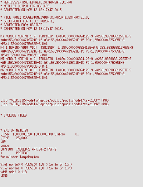
Hello all. I have been at this layout all day and I have seriously had it. So half way through the day I realized and confirmed that it is the source to body connection of the middle pmos that is missing (i think), the problem is I don't know how to make that connection! Simple, but I have tried every google search combination possible, there is absolutely nothing about this online! I will attach my layout and the netlists for comparison. Please any help will be much appreciated.

PS: I know my layout is poorly constructed.
EDIT: Forgot to mention, DRC is successful.
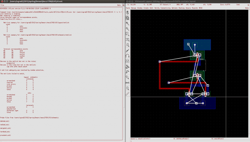
nor_layout.png

schem_netlist.png

extract_netlist.png
 
Engineering news on Phys.org
You simply need to extend the N-well (the green region, I think) in which the middle device sits until it touches the N-well in which the upper device sits. Since the upper N-well is contacted, this will contact the middle well also. As it stands, the middle N-well is floating. Alterantively, you could add another N-well contact region (the blue rectangle at the top) off to the right of the middle device. Make sure the middle N-well is tied to Vdd, not to the source of the middle device. Does this make sense?
 
  • Like
Likes 1 person
phyzguy said:
You simply need to extend the N-well (the green region, I think) in which the middle device sits until it touches the N-well in which the upper device sits. Since the upper N-well is contacted, this will contact the middle well also. As it stands, the middle N-well is floating. Alterantively, you could add another N-well contact region (the blue rectangle at the top) off to the right of the middle device. Make sure the middle N-well is tied to Vdd, not to the source of the middle device. Does this make sense?

Thank you so much for your reply. Finally an answer. In my schematic that middle pmos has its body connected to its source. If I extend the nwell of the middle pmos to the top pmos, won't that connect the body of the middle pmos to vdd? Or is the nwell not the body of the pmos? I will try to implement what you have said in a couple of hours. Once again, your help is much appreciated.
 
perplexabot said:
Thank you so much for your reply. Finally an answer. In my schematic that middle pmos has its body connected to its source. If I extend the nwell of the middle pmos to the top pmos, won't that connect the body of the middle pmos to vdd? Or is the nwell not the body of the pmos? I will try to implement what you have said in a couple of hours. Once again, your help is much appreciated.

Your schematic should not have that PMOS body connected to its source. In logic circuits, the PMOS bodies should all be connected to the most positive point (Vdd), and the NMOS bodies should all be connected to the most negative point(Vss), otherwise you run the risk of forward biasing the S/D junctions.

The N-well is the body of the PMOS devices. I suggest you connect those N-wells together and correct your schematic.
 
  • Like
Likes 1 person
phyzguy said:
Your schematic should not have that PMOS body connected to its source. In logic circuits, the PMOS bodies should all be connected to the most positive point (Vdd), and the NMOS bodies should all be connected to the most negative point(Vss), otherwise you run the risk of forward biasing the S/D junctions.

The N-well is the body of the PMOS devices. I suggest you connect those N-wells together and correct your schematic.

I didn't know that! Thank you! I will do so as soon as I can. I hope this will fix my error.

I kind of also have 1 more question which is kind of off topic. I have seen those fancy gate layouts online. They have like transistors lined up with there nwells connected (which now makes sense after ur explanation), my question is, do I need to construct such transistors myself following the drc rules or is there a way to merge to transistors that I have extracted from the schematic?
 
perplexabot said:
I didn't know that! Thank you! I will do so as soon as I can. I hope this will fix my error.

I kind of also have 1 more question which is kind of off topic. I have seen those fancy gate layouts online. They have like transistors lined up with there nwells connected (which now makes sense after ur explanation), my question is, do I need to construct such transistors myself following the drc rules or is there a way to merge to transistors that I have extracted from the schematic?

I don't really understand your question, but it probably depends on what you are trying to do. If you just want a circuit that works, what you have done is fine, but if you are building a commercial circuit and trying to make money on it you need the layout to be as efficient as possible, so that it takes up a minimum amount of area and runs as fast as possible. That's why those layouts are done that way.
 
  • Like
Likes 1 person
phyzguy said:
I don't really understand your question, but it probably depends on what you are trying to do. If you just want a circuit that works, what you have done is fine, but if you are building a commercial circuit and trying to make money on it you need the layout to be as efficient as possible, so that it takes up a minimum amount of area and runs as fast as possible. That's why those layouts are done that way.

Thank you for all your help. I will let you know if I still get errors after the fix.
 
perplexabot said:
I have seen those fancy gate layouts online. They have like transistors lined up with there nwells connected..


Could this be to increase drive strength if this transistor drives physical pin on device?
 
the_emi_guy said:
Could this be to increase drive strength if this transistor drives physical pin on device?

I don't know, that is why I am asking? I thought it was to make the design more compact. I am talking about when they use the same nwell and have multiple gates of polysilicon on that same nwell instead of having two isolated nwells with a gate for each.

Thanks
 
  • #10
You put the devices lined up sharing drains when possible to minimize area and optimize performance. Most layout tools (depending on the PDK) will either let you snap the device together (if you have the right setting selected) or you will have to overlap the drain areas yourself and make sure you don't have a DRC errors.

While phyzguy is right that your should source-well connect a PMOS in a logic circuit, if you wanted to for some reason (for example to adjust the threshold for power management) you can put that device in its own n-well and then put a n-well contact that is connected to the source. This will take some extra area because typically the well-to-well spacing rule in the design rules is pretty large.
 
  • Like
Likes 1 person
  • #11
analogdesign said:
You put the devices lined up sharing drains when possible to minimize area and optimize performance. Most layout tools (depending on the PDK) will either let you snap the device together (if you have the right setting selected) or you will have to overlap the drain areas yourself and make sure you don't have a DRC errors.

While phyzguy is right that your should source-well connect a PMOS in a logic circuit, if you wanted to for some reason (for example to adjust the threshold for power management) you can put that device in its own n-well and then put a n-well contact that is connected to the source. This will take some extra area because typically the well-to-well spacing rule in the design rules is pretty large.

That was exactly what I was asking about. Perfect answer. Thank you.
 
  • #12
phyzguy said:
You simply need to extend the N-well (the green region, I think) in which the middle device sits until it touches the N-well in which the upper device sits. Since the upper N-well is contacted, this will contact the middle well also. As it stands, the middle N-well is floating. Alterantively, you could add another N-well contact region (the blue rectangle at the top) off to the right of the middle device. Make sure the middle N-well is tied to Vdd, not to the source of the middle device. Does this make sense?

Thank you that fixed my error. Finally!
analogdesign said:
You put the devices lined up sharing drains when possible to minimize area and optimize performance. Most layout tools (depending on the PDK) will either let you snap the device together (if you have the right setting selected) or you will have to overlap the drain areas yourself and make sure you don't have a DRC errors.

While phyzguy is right that your should source-well connect a PMOS in a logic circuit, if you wanted to for some reason (for example to adjust the threshold for power management) you can put that device in its own n-well and then put a n-well contact that is connected to the source. This will take some extra area because typically the well-to-well spacing rule in the design rules is pretty large.

I just overlapped the drains (just as you said)! It Worked! Check this out! LVS AND DRC PASS! I went from that ugly thing in my OP to this beautiful creation : )

norFancy.png


Thank you all for your help.
 
  • #13
perplexabot said:
Thank you that fixed my error. Finally!


I just overlapped the drains (just as you said)! It Worked! Check this out! LVS AND DRC PASS! I went from that ugly thing in my OP to this beautiful creation : )

norFancy.png


Thank you all for your help.

Now that looks like a proper NOR gate!

Only a couple comments. Typically you wouldn't use long poly runs for your A and B inputs because poly is slow (high capacitance and high resistance compared to the metals).

How many metals do you have in your process? Typically you would try to make odd metals go in one direction and even metals go in the other. However that isn't necessarily a issue here because logic cells don't have to be routed out to the edges. In a practical digital circuit the logic cells are mashed together and then the metal routes come in from higher metal.

Looks good though. Those are minor suggestions. :)
 
  • #14
analogdesign said:
Now that looks like a proper NOR gate!

Only a couple comments. Typically you wouldn't use long poly runs for your A and B inputs because poly is slow (high capacitance and high resistance compared to the metals).

How many metals do you have in your process? Typically you would try to make odd metals go in one direction and even metals go in the other. However that isn't necessarily a issue here because logic cells don't have to be routed out to the edges. In a practical digital circuit the logic cells are mashed together and then the metal routes come in from higher metal.

Looks good though. Those are minor suggestions. :)

Thanks a lot for your feedback, will definitely consider when looking into my next layout.

I have another problem... I don't know if I should open a new thread of ask it on this one?! I will ask it here, I feel is better.

I made a layout for my inverter, it passed LVS and DRC. I then needed to make a buffer, so I used two of my inverters in series. However now it gives me a bunch of "Edge not on grid" DRC errors!

I thought that since my inverter passed the DRC test, so then must my buffer?
 
Last edited:
  • #15
Oh the dreaded grid. Are you using Cadence (your layout looks like Cadence but all the vendors copy Cadence these days)? If so you have to set the snap grid to the same setting that you used when you did the inverter layout.

Go to your virtuoso layout window and hit 'e'. THen set the X and Y snap spacing to 0.05 (that will probably work).

Then delete one of the inverters and instantiate it again. It should now be on grid. You might have to redo the wiring. Cadence is weird about the grid.
 
  • Like
Likes 1 person
  • #16
analogdesign said:
Oh the dreaded grid. Are you using Cadence (your layout looks like Cadence but all the vendors copy Cadence these days)? If so you have to set the snap grid to the same setting that you used when you did the inverter layout.

Go to your virtuoso layout window and hit 'e'. THen set the X and Y snap spacing to 0.05 (that will probably work).

Then delete one of the inverters and instantiate it again. It should now be on grid. You might have to redo the wiring. Cadence is weird about the grid.

Thanks for the quick reply. My snap grid settings are already the same for both my inverter and my buffer. And yes, I am using cadence.

EDIT: FIXED! Had to delete them and make two new instances (as you said).

Thanks for the help
 
Last edited:
Back
Top