Solving Op-Amp Current Analysis: LH0005 National Semiconductor

AI Thread Summary
The discussion revolves around solving a homework problem related to the LH0005 op-amp, specifically determining the collector current through each transistor. The user initially struggles with finding IC2 and receives guidance on analyzing the circuit, including the significance of VBE and the configuration of the transistors. Clarifications about node names and grounding lead to a better understanding of the voltage at the common emitter node, allowing for the calculation of currents through the transistors. Ultimately, the user successfully resolves the problem with the assistance provided, highlighting the importance of correctly interpreting circuit diagrams and voltage references. The conversation emphasizes the collaborative nature of troubleshooting in electronics analysis.
txp2037
Messages
5
Reaction score
0
Member advised to use the homework template for posts in the homework sections of PF.
Thank you for reading my post. I'm currently studying Op-amp, and there is a homework about LH 0005 of National Semiconductor for me to do: determine the collector current through each transistor

I'm trying to find the IC2 but don't know how. Please help me with this :)

Homework Statement


Given: β = 100 & VBE = 0.7

Homework Equations

The Attempt at a Solution


I tried to analyze but I'm stuck at the moment. Here are somethings that I've figured out so far:
VC2 = VCC - 10k*IC2
VE6 = VC2 - VBE6 = VC2 - 0.7
VC5 <<<
I2 = (VE2 + VEE) / 12k
I6 = (VE6 + VCC) / 2k

I'm trying to find the IC2 but don't know how. Please help me with this :)
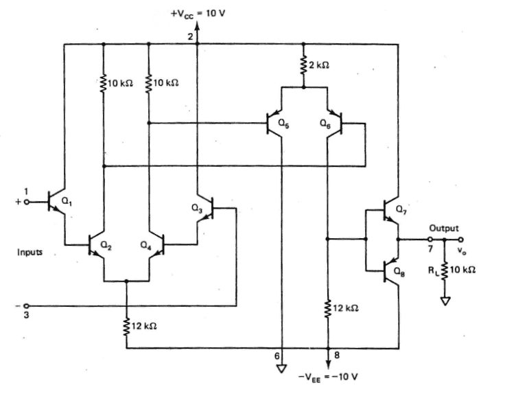
a1d0e395e0.png

I'm looking forward to seeing your response soon :)
 
Last edited by a moderator:
Physics news on Phys.org
Txp2037, you have overlooked that Q6 is pnp (VBE=-0.7V).
 
LvW said:
Txp2037, you have overlooked that Q6 is pnp (VBE=-0.7V).
Thank you for reminding me :) I'm struggling with the problem. By any chance you can give me some hints?
 
txp2037 said:
Thank you for reminding me :) I'm struggling with the problem. By any chance you can give me some hints?

Question: Are you required to find the quiescent collector currents for the shown input voltages?
This will create problems because - assuming VBE=0.7V as mentioned - the base potentials for Q1 and Q3 are equal.
However, this is in contradiction to the given signal voltages.
It is more likely that Q3 will be completely off. However, in this case, we are not in linear mode anymore.
Perhaps you should review the task again (with the dc input voltages)?
 
LvW said:
Question: Are you required to find the quiescent collector currents for the shown input voltages?
This will create problems because - assuming VBE=0.7V as mentioned - the base potentials for Q1 and Q3 are equal.
However, this is in contradiction to the given signal voltages.
It is more likely that Q3 will be completely off. However, in this case, we are not in linear mode anymore.
Perhaps you should review the task again (with the dc input voltages)?
Thank you for your reply. My requirement are (and I quote): Referring to the LH0005 op-amp equivalent circuit shown in figure, determine (a) the collector current through each transistor and (b) the de voltage at the output terminal. (Assume that each transistor has βdc = βac = 100 and VBE = 0.7 V.)
I think I can sort the (b) out, but I don't know how to find the collector current. I've written down some equations so when I know the IC2, I can solve the problem. About the input voltage, there are nothing given :)
 
Oh sorry - I have misinterpreted the drawing. So "1" and "3" are node names and not two different input voltages.
Therefore, I now assume that both open base terminals are grounded, correct?

In this case, it is a simple task to find the voltage at the common emitter node (because of VBE=0.7V for each transistor). This allows to compute the current to the emitter resistor (12k) - and the current is equally splitted between both transistors Q2 and Q4.
 
LvW said:
Oh sorry - I have misinterpreted the drawing. So "1" and "3" are node names and not two different input voltages.
Therefore, I now assume that both open base terminals are grounded, correct?

In this case, it is a simple task to find the voltage at the common emitter node (because of VBE=0.7V for each transistor). This allows to compute the current to the emitter resistor (12k) - and the current is equally splitted between both transistors Q2 and Q4.
You gave something awesome here. So as you said, the VB1 will be 0V. Then VE1 = VB1 - VBE1 = 0 - 0.7 = -0.7V.
VE1 = VB2 = -0.7V ==> VE2 = VB2 - VBE2 = -1.4V
Then I can find the I2 = 2IE2 = (VE2 + VEE) / 12k = (-1.4 + 10) / 12k =~ 0.717mA.
Am I currently on the right way?
 
txp2037 said:
Then I can find the I2 = 2IE2
I rather think that I2=IE/2.
 
  • Like
Likes txp2037
LvW said:
I rather think that I2=IE/2.
Thank you for your help. Under your guide, I've managed to solved the problem completely :) I was misunderstood about the "ground" voltage that should be 0V. With that information, everything was clear :) Thank you sir
 
  • #10
Could you further elaborate how voltage gain, Ri etc are calculated...
 
Back
Top