MarcL
- 170
- 2
Tried using the template, had to put pictures because this concerns a diagram question! sorry guys!
1. Homework Statement
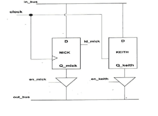
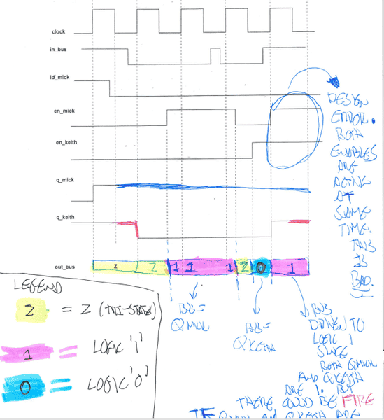
Consider the circuit shown in the figure below which consists of a positive edge triggered flipflop with selective load capability (identified as MICK) and a level sensitive D-type latch (labelled as KEITH). There is an input bus (consisting of a single wire) , an output bus, and two tri-state buffers. Complete the timing diagram which is included at the end of this question. Indicate in the provided timing diagram the behavior of the output of the flip-flop and the latch (q_mick and q_keith) as well as the behavior of the output bus between the indicated “start” and “end” times. Use the symbol “Z” to denote the state of the output bus when it is in the high impedance (tri-state value). In the given diagram, it is assumed that the initial value of q_mick is logic ‘0’ and that the initial value of q_keith is logic ‘1’. Note also that the timing diagram intentionally contains a fatal design error. You are to explain in words the nature of this design error. Use the word “FIRE” in the appropriate place in the timing diagram to indicate the state of the output bus at the interval in time during which the design error occurs.
Diagram:

Timing diagram to complete:

Answer ( which I do NOT understand, the answer itself and don't even get me started on the handwritting! haha):

I really don't think I need equations in this problem
I can't even answer the question, not even a bit, I have so many questions concerning the question itself:
1) positive edge triggered flipflop with selective load capability --> what is that? I mean it is triggered on rising edge but selective load capability? I don't know what that stands for.
2) level sensitive D-type latch --> I know what a D-type latch is but "level sensitive"? I mean I've never hear of that too ( is it even relevant to the problem?)
3) Also if MICK is positively triggered, why doesn't it fall on the falling edge of the clock?
4) As for the q_keith, why is it only triggered when the input is turned to 1? I thought, again it would trigger with the clock ( I have a feeling I'm mixing up a concept here)
5) I know a tri-state buffer "buffs" the current ( hence the name - unless I'm wrong). But how do you know whether or not "the output bus when it is in the high impedance"? Does it just mean when the output is 1?
6)Why can't en_mick/keith be both enabled at the same time? I thought they are both different output so they can behave differently.
7) what on Earth is id_mick? Is it even relevant to the question?
Sorry for the long question guys
1. Homework Statement
Consider the circuit shown in the figure below which consists of a positive edge triggered flipflop with selective load capability (identified as MICK) and a level sensitive D-type latch (labelled as KEITH). There is an input bus (consisting of a single wire) , an output bus, and two tri-state buffers. Complete the timing diagram which is included at the end of this question. Indicate in the provided timing diagram the behavior of the output of the flip-flop and the latch (q_mick and q_keith) as well as the behavior of the output bus between the indicated “start” and “end” times. Use the symbol “Z” to denote the state of the output bus when it is in the high impedance (tri-state value). In the given diagram, it is assumed that the initial value of q_mick is logic ‘0’ and that the initial value of q_keith is logic ‘1’. Note also that the timing diagram intentionally contains a fatal design error. You are to explain in words the nature of this design error. Use the word “FIRE” in the appropriate place in the timing diagram to indicate the state of the output bus at the interval in time during which the design error occurs.
Diagram:
Timing diagram to complete:
Answer ( which I do NOT understand, the answer itself and don't even get me started on the handwritting! haha):
Homework Equations
I really don't think I need equations in this problem
The Attempt at a Solution
I can't even answer the question, not even a bit, I have so many questions concerning the question itself:
1) positive edge triggered flipflop with selective load capability --> what is that? I mean it is triggered on rising edge but selective load capability? I don't know what that stands for.
2) level sensitive D-type latch --> I know what a D-type latch is but "level sensitive"? I mean I've never hear of that too ( is it even relevant to the problem?)
3) Also if MICK is positively triggered, why doesn't it fall on the falling edge of the clock?
4) As for the q_keith, why is it only triggered when the input is turned to 1? I thought, again it would trigger with the clock ( I have a feeling I'm mixing up a concept here)
5) I know a tri-state buffer "buffs" the current ( hence the name - unless I'm wrong). But how do you know whether or not "the output bus when it is in the high impedance"? Does it just mean when the output is 1?
6)Why can't en_mick/keith be both enabled at the same time? I thought they are both different output so they can behave differently.
7) what on Earth is id_mick? Is it even relevant to the question?
Sorry for the long question guys