Understanding Comparator and Window Comparator Functionality in Op-Amps

Click For Summary
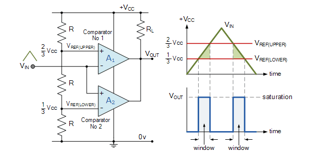
The discussion focuses on the functionality of comparators and window comparators in op-amps, particularly the behavior of outputs when input voltages cross specific thresholds. When Vin exceeds 2/3 Vcc, the first comparator activates, leading to a negative output, while the second comparator should also activate due to Vin being above 1/3 Vcc, causing confusion about which output takes precedence. The circuit's design allows for a "wired-AND" configuration, where the output is high only if all comparators are high, and low if any comparator is low. The conversation also clarifies the concepts of sourcing and sinking current, emphasizing that certain outputs can only sink current and cannot source it. Understanding these principles is crucial for effectively utilizing op-amps in circuit design.
jaus tail
Messages
613
Reaction score
48
Hi,
While studying opamps I came across comparator and window comparator.
upload_2016-12-23_12-54-10.png

I had trouble understanding case of Vin > 2/3 Vcc.

As per waveform, comparator 1 is functional and o/p goes negative.
But isn't now Vin also more than 1/3 Vcc, so shouldn't comparator 2 make o/p positive.

Also when Vin < 1/3 Vcc, then as per waveform, comparator 2 is active and o/p goes negative,
but now isn't comparator 1 also active as Vin is also less than 2/3 Vcc, so o/p can also go positive.

How does the circuit know which opamp to follow?
 

Attachments

  • upload_2016-12-23_12-53-57.png
    upload_2016-12-23_12-53-57.png
    73.3 KB · Views: 776
Engineering news on Phys.org
It seems that comparators A1 and A2 have outputs which when LOW can sink current (to ground) but when HIGH do not source current, but merely present an open circuit (high impedance or off) at the output. In TTL logic this was known as an open-collector output.

The practice of connecting together multiple outputs is generally not encouraged. Here, it could be termed a "wired-AND" gate, meaning their common output is HIGH only if all the comparators are driven HIGH. If even one output is LOW then the wired connection will go LOW.

https://www.physicsforums.com/attachments/holly-1756-gif.110502/
 
Last edited:
  • Like
Likes jaus tail
NascentOxygen said:
The practice of directly connecting outputs is generally not encouraged. Here, it could be termed a "wired-AND" gate, meaning their common output is HIGH only if all the comparators are driven HIGH. If even one output is LOW then the wired connection will go LOW.

[PLAIN]https://www.physicsforums.com/attachments/holly-1756-gif.110502/[/QUOTE]
Thanks for this.
 
Last edited by a moderator:
Look on datasheets for terms "Open Collector" and "Wired Or" . It's not uncommon, and that's why they make "open collector" logic ICs.

http://www.ti.com/lit/ds/symlink/sn7406.pdf
upload_2016-12-24_9-29-21.png


observe Output pin can only accept(sink) current.
A 555 timer's Discharge pin is open collector. A single 555 package could do the job of your schematic in post 1.
 
  • Like
Likes NascentOxygen
jim hardy said:
Look on datasheets for terms "Open Collector" and "Wired Or" . It's not uncommon, and that's why they make "open collector" logic ICs.

http://www.ti.com/lit/ds/symlink/sn7406.pdf
View attachment 110750

observe Output pin can only accept(sink) current.
A 555 timer's Discharge pin is open collector. A single 555 package could do the job of your schematic in post 1.

Thanks for the reply. I'm confused about source and sink currents. In your picture how can output Y be sink current. Collector current will flow from Y ti the BJT. It can't flow in reverse direction for npn transistor.
i got this diagram from the internet for source and sink currents.
upload_2016-12-24_22-48-16.png


Link of pictures.
http://electronicsbeliever.com/what-is-source-and-sink-current/
 

Attachments

  • upload_2016-12-24_22-47-7.png
    upload_2016-12-24_22-47-7.png
    8.8 KB · Views: 689
The output Y is able to conduct current (conventional flow) into the collector of the transistor and through the transistor to ground. The transistor when turned on is a switch to ground. It cannot source current. There is no switch to Vcc. The diagrams you posted are confusing you as they talk about currents prior to the output transistor which is not relevant to this discussion. The link posted by jim hardy in post #4 does not have any way to connect to anything that is anywhere connected to an output except Y. So why concern yourself with any currents in any transistor other than at the terminal Y?
 
  • Like
Likes jaus tail and jim hardy
jaus tail said:
I'm confused about source and sink currents.

Vocabulary question not physics question. Your link answered it, even if not succinctly.

As Averagesupernova said,
once you accept that current is positive charge in motion it's obvious -
Sourced current comes OUT of a terminal, just like water from a spigot,
and Sunk current flows INTO a terminal just like water down the drain.

A Source delivers current,
a Sink accepts it.

look up 555 datasheet - the OUT pin can both source and sink, DIS pin only sinks.
 
Last edited:
  • Like
Likes jaus tail and Averagesupernova
jaus tail said:
In your picture how can output Y be sink current.
Y can conduct current to ground—but only if the load is an external impedance connecting to +Vcc , similar to the arrangement in post #1.

If you were to connect a load between Y and ground, you can see that current could never flow through the load: when Y is HIGH or open-circuit there would [obviously] be zero load current, and when Y is LOW there would be zero load current, so it is useless to connect an external load between Y and ground. Y cannot supply current to a load, Y can only absorb current from the load.

https://www.physicsforums.com/attachments/110502.gif
 
  • Like
Likes jaus tail
NascentOxygen said:
Y can conduct current to ground—but only if the load is an external impedance connecting to +Vcc , similar to the arrangement in post #1.

If you were to connect a load between Y and ground, you can see that current could never flow through the load: when Y is HIGH or open-circuit there would [obviously] be zero load current, and when Y is LOW there would be zero load current, so it is useless to connect an external load between Y and ground. Y cannot supply current to a load, Y can only absorb current from the load.

[PLAIN]https://www.physicsforums.com/attachments/110502.gif[/QUOTE]

Thanks for this.

jim hardy said:
A Source delivers current,
a Sink accepts it.

look up 555 datasheet - the OUT pin can both source and sink, DIS pin only sinks.

Thanks for the definition. So a battery is source whereas any load is sink.
 
Last edited by a moderator:

Similar threads

Replies
80
Views
5K
Replies
5
Views
3K
  • · Replies 5 ·
Replies
5
Views
3K
  • · Replies 12 ·
Replies
12
Views
3K
  • · Replies 3 ·
Replies
3
Views
2K
  • · Replies 20 ·
Replies
20
Views
5K
  • · Replies 7 ·
Replies
7
Views
6K
  • · Replies 33 ·
2
Replies
33
Views
13K
  • · Replies 6 ·
Replies
6
Views
8K
  • · Replies 15 ·
Replies
15
Views
5K