Where is the demodulator in this AM receiver?

AI Thread Summary
The discussion revolves around building an AM receiver and identifying the demodulator within the circuit. Participants clarify that the 500 pF capacitor and 200 µH inductor form a parallel LC circuit tuned to the receiving frequency, while the first two transistors likely create a Darlington pair for audio envelope detection. There is debate about the role of the third transistor, Q3, which may serve dual purposes of demodulating the RF carrier and amplifying the audio signal. Concerns are raised about the circuit's biasing and feedback stability, with suggestions for adjusting component values to improve performance. Ultimately, the base-emitter junction of Q3 is proposed as a potential demodulation point due to its non-linear characteristics.
Boltzman Oscillation
Messages
233
Reaction score
26
TL;DR Summary
I do not see a modulator on this receiver. Can anyone let me know where it is?
I am trying my hands on building receivers and transmitters. For now I would like to build this receiver here:
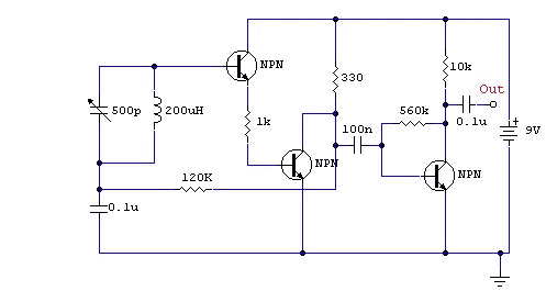
1594249828830.png

now I see that the 500pH inductor in parallel witht he 200uH capacitor are in charge of filtering the unwanted frequencies. The top-left NPN is in my guess an emitter follower to prevent loading? I've no idea what the middle NPN is for. I also have no clue what the right-most NPN is for but my guess is as an amplifier simply because I assume every radio needs an amplifier of some sort (I am probably wrong). The demodulators I am used to seeing are the ones that use diodes. Now since BJTs are sort of like diodes then I assume that you can possibly use them for demodulation as well? I don't know really. Any help is appreciated.
 
  • Like
Likes Delta2
Engineering news on Phys.org
Boltzman Oscillation said:
now I see that the 500pH inductor in parallel witht he 200uH capacitor are in charge of filtering the unwanted frequencies.
Not quite... The 500 pF variable capacitor is in parallel with a fixed 200 uH inductor.

That parallel LC circuit is tuned to resonanate at the receive frequency.

The inductor is probably also being used as the antenna.

I believe the first two transistors form a low frequency darlington pair that detects the audio envelope of the RF.
 
  • Like
Likes hutchphd and Delta2
Baluncore said:
I believe the first two transistors form a low frequency darlington pair that detects the audio envelope of the RF.
I'm not sure how a Darlington pair would do envelope detection, but I could be missing the obvious. Also, the feedback is confusing me a bit.

@Boltzman Oscillation -- please always post links to your figures and quotes (unless you already did and I'm missing it).
 
https://www.eeweb.com/extreme-circuits/circuit-project-am-receiver
Description:
This is a compact three transistor, regenerative receiver with fixed feedback. It is similar in principle to the ZN414 radio IC which is now no longer available. The design is simple and sensitivity and selectivity of the receiver are good.

Notes:
All general purpose transistors should work in this circuit, I used three BC109C transistors in my prototype.The tuned circuit is designed for medium wave. I used a ferrite rod and tuning capacitor from an old radio which tuned from approximately 550 - 1600kHz. Q1 and Q2 form a compund transistor pair featuring high gain and very high input impedance. This is necessary so as not to unduly load the tank circuit.
The 120k resistor provides regenerative feedback,between Q2 output and the tank circuit input and its value affects the overall performance of the whole circuit. Too much feedback and the circuit will become unstable producing a "howling sound". Insufficient feedback and the receiver becomes "deaf". If the circuit oscillates,then R1's value may be decreased; try 68k. If there is a lack of sensitivity, then try increasing R1 to around 150k. R1 could also be replaced by a fixed resisor say 33k and a preset resistor of 100k. This will give adjustment of sensitivity and selectivity of the receiver.
Transistor Q3 has a dual purpose; it performs demodulation of the RF carrier whilst at the same time, amplifying the audio signal. Audio level varies on the strength of the received station but I had typically 10-40 mV. This will directly drive high impedance headphones or can be fed into a suitable amplifier.
 
  • Informative
  • Like
Likes Jody and berkeman
I ran across this, C1 L1 forms the tank circuit. Q1 is just a buffer. Q2 is just a gain stage. Q2 using Q1 to form a DC bias circuit for Q2 to operate. I put in the approx voltages. R2 and C2 form a low pass filter to create the DC bias of about 1.5V at the base of Q1 which gives about 0.7V at base of Q2. You can see the approx DC voltage at different points.

I don't see the demodulate circuit as C3 is just an AC coupling capacitor, it is like a high pass filter. I just see Q3 forms a second gain stage.

This is really old style circuit that I only saw in really old books, the bias is at the mercy of the beta, it is very inaccurate. I wrote the approx gain in green.
Radio.jpg
 
Last edited:
You do need some non-linear function to demodulate AM, so looking for a diode is a great guess. I'm too lazy to analyze this one, but I think @Baluncore must be correct, the darlington stage is probably clipping or saturating and doing the detection.
 
Q2 sure don't have a lot of headroom to swing, you can see the collector is sitting about 2V at best, it does not have much room to go lower. I don't know that can rectify the signal. I would expect some sort of low pass filter to get rid of the RF. there's none. R2 C2 is way way too slow for anything other than serving as DC bias.
 
yungman said:
This is really old style circuit that I only saw in really old books, the bias is at the mercy of the beta, it is very inaccurate.
Gain and coupling are corrected by adjustment of the 120k feedback resistor.
This is a regenerative circuit, so you must model it as an amplifier with high-pass feedback that almost oscillates. The low-pass bias will be dependent on signal strength. Think of the bias envelope as providing the audio output.

Regenerative and super-regenerative receivers can be incredibly sensitive and selective, with a minimum component count. That is why they are seen in old books. Components are now so cheap that component count is irrelevant and receivers must be easy to use by the unskilled listener.
https://en.wikipedia.org/wiki/Regenerative_circuit

My first receiver was a crystal set with one germanium diode. My second was a three tube super-regenerative, one vacuum tube did all the RF, another was the audio amplifier, the third was a full wave power rectifier.
 
  • #10
120K with 0.1uF?! the corner frequency is 1/(2pi x 120K x 0.1uF) = 13.3Hz. How is this have anything to do with RF? I don't get it. It is a low pass just to set up the DC bias for Q1 and Q2. At 130Hz, you can ignore the 120K and just the 0.1uF capacitor. I hope when we say RF, that's over 100KHz. At 100KHz, the reactance of 0.1uF is 15.9ohm. With the 120K resistor as voltage divider, I am pretty comfortable you can ignore the feedback from the 120K resistor,
 
  • #11
yungman said:
... , the bias is at the mercy of the beta, it is very inaccurate. ...
I believe you were complaining that the front-end bias was at the mercy of the darlington beta.
The 120k and 0u1F is correcting for that. The circuit note advises changing the value from 120k if there is not enough headroom. The bandwidth of the bias control must be sub-audio or it will cut the low frequencies.

There is also stray capacitive and inductive coupling everywhere in that front-end, including the antenna coil and the power supplies.
 
  • #12
Baluncore said:
I believe you were complaining that the front-end bias was at the mercy of the darlington beta.
The 120k and 0u1F is correcting for that. The circuit note advises changing the value from 120k if there is not enough headroom. The bandwidth of the bias control must be sub-audio or it will cut the low frequencies.

There is also stray capacitive and inductive coupling everywhere in that front-end, including the antenna coil and the power supplies.
Actually I was thinking about Q3 that using the base current to set up the voltage across the 560K that set the collector voltage. Any change of beta change the collector voltage. I assume the output voltage at collector Q2 is still small, don't need a lot of room to swing, but amplified by Q3, the voltage at collector has to be more significant. To increase headroom for Q2, increase R3 can do this too. creat more voltage drop across R3 to raise the collector voltage of Q2. Either way, it again depends of the base current of either Q1 or Q2, which is unreliable.

At less than or about 1MHz, stray inductance and capacitance should not be very important as the circuit is not very high impedance. When I think RF, it's like at least 100MHz to GHz and beyond. But of cause, if it is like the radio in the older days that use pcb without ground plane, components were standing up so one lead was long and all, that might introduce unforeseen issue. AND people don't have a habit of bypassing the power supply.

I still don't get where is the demodulator is.
 
  • #13
yungman said:
I still don't get where is the demodulator is.
The base-emitter junction of Q3 is a possible candidate. It is non-linear and the input is modulated by low impedance RF.
 
Back
Top