Boost converter switch node spiking

In summary: something else.scope trace is (presumably) when the switch is closed, inductor current is 0, overshoot happens when it's open
  • #1
Artlav
162
1
Greetings.

I'm making a high power boost converter, supposed to deliver constant current at 15-50V from about 12V input. 100KHz frequency.
xb-sch2.png

There are problems, however.

There was a lot of ringing at the switch node - meeting point of the diode, inductor and MOSFET.
5.8Mhz clear decaying sine wave, got rid of the most of it with an RC snubber - 5Ω, 10nF.

There is still, however, a big peak at the moment the switch closes.

15.5V 7.75A out, 12V 10A in (20V vertical)
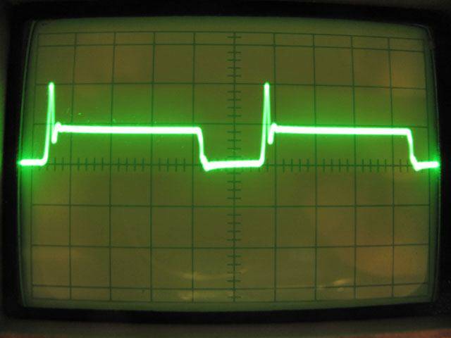
bc-10a.jpg


21V 10.5A out, 20A in.
The spike is already at nearly 60V.
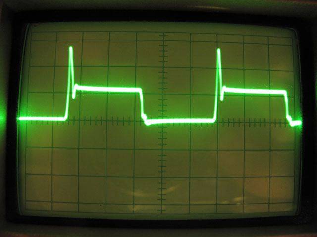
bc-20a.jpg


At this rate the spike will exceed the 100V rating of the transistor well before the 100A maximum input current i was aiming for.
There is a TVS diode across it, but i doubt it would help much to prevent the explosion.

Is there any way to get rid of this spike?
I suspect the devil is in the layout, but I'm not good enough to determine just what it is.

Here is what it looks like, input on the right, output to the left:
http://orbides.1gb.ru/img/bc-side.jpg
http://orbides.1gb.ru/img/bc-top.jpg

I tried moving the wires around, with no noticeable effect, and there is not much i can do to shorten the wires.
The MOSFET package is claimed to be "Low internal inductance", so that parasitic inductance must come from somewhere else, right?
 
Engineering news on Phys.org
  • #2
The diode needs to be a schottky diode. It is creating the spike when the switch opens. At that point the inductor slews to whatever voltage it needs to maintain its current. Since a normal switching diode has stored charge, it takes time for the diode to turn on. The other problem with non schottky diodes is that they appear as a momentary short when they are reverse biased (huge current spike through diode when the switch turns on)
 
  • #3
meBigGuy said:
The diode needs to be a schottky diode.
Does not seem to help much.
Placing another diode in parallel with the existing one reduces the spike ever so slightly, but actually replacing the existing one with a schottky (40CPQ060 to be exact) makes the spike worse.

There is a slight reduction of the spike if i screw the existing diode directly onto the MOSFET without the wire, but it's only about 5% or so.

Also, the spike happens when the switch closes, not when it opens.

meBigGuy said:
The other problem with non schottky diodes is that they appear as a momentary short when they are reverse biased (huge current spike through diode when the switch turns on)
40ns reverse recovery time on this one, you can't do much better than that.
 
  • #4
I'm confused then with respect to what your scope trace is. I assumed it was the voltage at the switch-inductor-diode junction. When the switch is closed that voltage is 0, then it jumps to the output voltage when the switch is opened. It then collapses (with ringing you suppressed with the snubber) to zero when the inductor current dies out. When it jumps to the output voltage it overshoots because the diode doesn't turn on right away (or some oither problem).

One way to determine whether wiring is affecting this is to move the ground trace of the scope. If you get radically different spikes grounded at the output vs grounded at the input the there is a layout problem. (or measure voltage from input ground to output ground)

Another very real possibility is that the inductance of the output capacitor is too high. Is it a low esr capacitor (very important)? Try a 100uF low esr capacitor and a 2.2uF ceramic in parallel with the 6800uF output capacitor. What spiking do you see on the output capacitor itself? If it shows no spiking then that is not the issue.
 
  • #5
The traces above are measured across the mosfet, with probe and ground connected directly to it's bolts.
Assuming switch=mosfet, the voltage is at the output level when it's closed, and drops to zero when it conducts.
As the switch closes there is a spike.

The ringing was that spike being a decaying sine wave.
The current should not die out - it runs in continuous mode at any interesting load.Moving the ground around do not produce any drastic changes.

Across the output capacitor there is a bit of bursts of ringing, +-1V or so, coinciding with opens and closes, it does seem to reduce if i add various small capacitors to it.
 
  • #6
We are confusing electrical terms. When the mosfet conducts == it is on == the switch is closed. When the mosfet turns off == the switch is open == mosfet doesn't conduct. That is pretty much the standard terminology.

So, the spike is definitely caused by the inductor trying to maintain its current when the mosfet stops conducting. If there is no comparable spike on the output capacitor, then the voltage is across the diode and is caused by the diode not turning on fast enough. You can prove this by slowing down the turn-off (non-conduction) of the mosfet. But be careful. If you slow it too much it will fry since the currents are so high.

You never mentioned the timebase of the waveforms.
 
  • #7
Maybe you need a faster diode, although I'd expect the schottky you tried to be fine. Try the Vishay TMBS series. They are optimized for high frequency.

If the lead inductance of the diode is the issue you will again see different voltages at the diode leads (input and output). But, I expect it is just too much too fast for the diodes you have chosen (although I really don't see a problem with your choices).

You could try a capacitor across the diode just to see what it does to the spike.

I haven't worked with switching currents as large as you are dealing with.
 
  • #8
Ah, sorry about the confusion - english is not my primary language.
Traces are at 2us, 20V per division.

I never seen forward turn on time mentioned in diode datasheets.

I tried 40CPQ060 schottky and 10sq045 schottky barrier - both reduce the spike ever so slightly if placed in parallel to the big one, and increase the spike if placed instead of it.
So, either these are just as bad or there is something more going on there.

One thing i can think of is using synchronous rectification, but i have no clue how to find the right IC for the job.
 
  • #9
meBigGuy said:
You could try a capacitor across the diode just to see what it does to the spike.
Now, that did something.

Things started happening at 100nF, film cap across the diode.

Before:
FET, 2us, 10V.
bc-fet-before.jpg

Output, 2us, 1V.
bc-out-pre.jpg


After:
FET, 2us, 10V.
bc-fet-after.jpg

Output, 2us, 1V.
bc-out-after.jpg


Not all the way, making different oscillations, and heating the capacitor noticeably, but feels like progress.
Is there any theory behind what capacitor to choose, and how much heat to expect on it?

And where can that new ringing be coming from?
 
  • #10
One more thing - it's the ESR/ESL of the capacitor that matter, not it's value.
Same 100nF, but as a quality X2 capacitor:
bc-fet-after-x2.jpg


Looks almost perfect, spike-wise.
However, i don't like that low frequency ringing that is now all over the place.
 
  • #11
The problem is the turn on time of the diode is too slow. When the FET turns off the inductor must still conduct. But there is a finite amount of time for the diode to go from non conducting to conducting. So the inductor just keeps pushing charge into Cj of the diode until it can be drained out. Because Cj is small and I is large there is a lot of V. (You can confirm this experimentally by varying the Idc in the L and observing the peak change. If you have a load R vary it.) By putting a cap in parallel with the diode you increase the C but Q stays basically the same so there is less V. (Note: you have to be able to access the C. If there is excessive ESR or ESL the C cannot be accessed by the high frequency I induced by the switch.)

In general this is not a preferred way to damp the peak compared to a switch node RC snubber because I think you'll notice the efficiency of the conversion just went way down.

The snubber should've worked. It's purpose is also to provide an escape path for the inductor current while the diode is turning on (some people think of it as an AC short, or damping the LC, its all just different sides of the same coin in my opinion).

Try using this technique to pick the snubber RC with the Schottky. I've used it plenty of times and it always works for me.
http://www.ti.com/lit/an/slva255/slva255.pdf
 
Last edited:
  • #12
I just looked at the images of the converter you constructed. It's actually kind of beautiful in my opinion. But you'll never going get the parasitics down low enough in that setup for these switch times. You're definitely going to need the snubber.
 
  • #13
eq1 said:
Try using this technique to pick the snubber RC with the Schottky. I've used it plenty of times and it always works for me.
http://www.ti.com/lit/an/slva255/slva255.pdf
That's exactly the article i used to pick the snubber.
It worked, turning a raging ringing into a little spike.
But that little is still a lot.

eq1 said:
In general this is not a preferred way to damp the peak compared to a switch node RC snubber because I think you'll notice the efficiency of the conversion just went way down.
Hardly way down - the capacitor barely heats at all, and the efficiency remain around 85-90% all the way into KW range.

What troubles me is what this capacitor adds.
The spike is not actually removed completely by it - it is reduced, but on top of that there is a new wave in there, and a spike that follows it.

Can't quite describe it, so here is a video.
Input going from 10A to 75A, then back down (AFAIK the switching current ripples +-5A from input one, based on F and L used).
20V/2us per division, across the MOSFET
https://www.youtube.com/watch?v=mHgYDOsXigA

It's still getting uncomfortably close to the breakdown voltage, and now it's not a mere spike, but a big wide interval.
 
  • #14
I have a problem with the schottky diodes behaving worse. Makes me think it is inductive effects of your wiring.

Adding a capacitor across the diode is not really an acceptable solution. I just suggested it to see if it, by providing a path for the inductor current, verified that the problem is the diode turn on. But it has other side effects that mask the data.

With the capacitor in the circuit you now have a series resonance which is causing a sine wave superimposed on the current ramp. As that beats with the controller it sometime switches when current is low, and sometimes when current is high, therefore sometimes no spike, sometimes huge spike.

I suggest the following:
1. With the probe ground in 1 place (at the input or mosfet ground), probe *all* points in the circuit and see if any spiking is caused by ground or lead inductances. The reason I suggest this again is that a schottky is supposed to have no reverse recovery time. If that is the case, then wire inductances in your free-air layout must be causing the spiking. The diode has a specified inductance. How does that jive with the spike you are seeing. Probe both sides of the diode as close as possible to the package. If the spike is less on the input side, then it is the lead inductance. You are looking for any changes across a wire. Again, probe both sides of all wires.

2. Slow down the turn-off time of the mosfet. This will increase the power in the mosfet, but give the current a place to go while the diode turns on. It will reduce the spike.

3. Go to sync rectifier, as you stated.
 
  • #15
In addition to what mrBigGuy said, maybe try moving the snubber. From the pictures I think it is connected directly across the DS of the FET. This means the snubber and FET are sharing a return current to the input cap in that heavy wire. There can be ~150A in that wire so even a small ESL there will make a big difference. Maybe try removing that snubber cap from the S of the FET and connect it to the input cap ground directly in its own wire. Do your best to keep the snubber wire length as short a possible.

Also, make sure the snubber has a low ESR and ESL cap in it as well.
 
  • #16
You might also try adding the Cout-byp that the TI app note recommends. Connect it directly to the cathode of the diode and give that cap it's own wire to the ground pin of the input cap as well. Again, do your best to keep that wire short and use a low ESL cap if possible. The 100nF thin film will probably work well.
 
  • #17
Actually, the more I think of it the more I think it is inductive effects at your high currents. I just don't think a schottky forward recovery time can be that large, and using shottky made it worse (which could have been wire related)

V= Ldi/dt
To get 50V in 300ns given 50A only requires 300nH. 1 inch of straight wire in free space is about 40 to 50nH. (http://www.consultrsr.com/resources/eis/induct5.htm has a calculator)

You can decrease inductance by going to wide braided wire, multiple wires, using a ground plane or by shorter wires.

I really think you should be able to see the spike levels change as you probe different points.

Do you plan to lay this out? If not, maybe you should build it on a sheet of heavy copper covered pcb material
 
  • #18
A capacitor across the diode appear to only be effective at lower power - higher up it gets overwhelmed by the trapezoidal peak.

Moving the snubber to input ground makes a bit of a difference, but not really significant. Having two snubbers - one on DS, other D to input ground seems better than either alone.
High frequency noise on the diode is cleaned up by adding an RC snubber across it - 3300pF, 15Ω. That one also contribute a few percent reduction to the spike.
Changing all snubber caps to MKP X2 shaves off another percent or two.

The biggest effect, however, is adding a capacitor from the output end of the diode straight to the input ground - 2uF MKP X2. That reduces the spike at the MOSFET about as well as the capacitor across the diode did, but without additional ringing. The bigger this one is - the better, but above 1-2 uF it no longer change much.

Bad news about it is - at high power it heats a lot, and the spike turns into a full scale calamity.
20V/2us per division, across the MOSFET, 10A to 80A input:
https://www.youtube.com/watch?v=FJG2j0JfTXI

To me that looks worse than the ringing with a cold capacitor across a diode.

For the reference, here what it looks without anything at the diode.
20V/2us per division, across the MOSFET, 10A to 50A input:
https://www.youtube.com/watch?v=_9-fS9Ljiaw

So ultimately, all these diode shenanigans are quite pointless at anything above the lower power levels.
It seems to me that there are two spikes superimposed over each other - one is small, and is filtered out by various ways of putting a capacitor on a diode, and the other is big and growing with power, and is not affected by anything i do.

meBigGuy said:
Do you plan to lay this out? If not, maybe you should build it on a sheet of heavy copper covered pcb material
I was expecting current layout to be final, but it seems like there is no fixing it like it is.
Any advice on how to lay it out? I can't quite visualize it on a PCB when even 4mm wires are warming up.

I do have a 2mm thick sheet of copper, so maybe use it as a ground plane, and mount everything in it's line?
Kind of like this:
xb-nlay.png


meBigGuy said:
Go to sync rectifier, as you stated.
Any advice on what sort of IC to look for?
 
  • #19
Your input capacitor at 100,000 uF is unnecessarily huge with lots of inductance. I am surprised it is needed. Surely 1000 uF would be more than enough. If your input leads are very long then a Pi input filter should be a better investment as it will offer lower impedance at the switching frequency.

The 6800 uF output capacitor is much too inductive for that application. It needs to be paralleled with a small fast high current capacitor to catch the switching edge. Big capacitors are not better for spikes, they are far worse. Big capacitors are good for ripple. Use two different capacitors for the best of both worlds.

Since the transition that causes the problem involves only the 20 uH inductor and the fast diode the best way to snub the spike is to put a capacitor across both those components. That would be between the (+)input and (+)output and would divert the spike from the ground inductance into a much smaller current loop. The capacitor need only handle the spike so an 0.1uF disc ceramic, possibly in parallel with a metallised polypropylene suppression capacitor should eliminate most of that spike.
 
  • #20
Re: Metallized Polypropylene Film Capacitors.

Take a look at the table in this document;
http://www.cde.com/catalogs/935.pdf
You will see ripple current specified in the table.

13A, 48V output suggests an input current from a 12V supply of about 50A flowing through the inductor and diode.
You will need a few small caps in parallel as your spike catcher and/or output filter.
They are available from Digikey in USA.
 
  • #21
I'm convinced that your problem is not diode turn on time when you are using a shottky. It is wiring inductance. A sync recitifier will not help that problem.

Can you explain why a capacitor from the diode output to input ground would have any effect? It is just in parallel with the output capacitor. It should be no different than putting it in parallel with the output capacitor. (except for the ground wiring! <----------- very important). You stated previously that capacitors across the 6800uF had little effect (which is hard to accept).

You still have not stated that you have put the scope ground in 1 place (preferrably the input ground terminal) and then measured the spikes at both ends of all wires.

You need to get a handle on the currents that are flowing and the inductances of the wires.

1. Low ESR, low inductance output capacitor utilizing multiple capacitors. 1uF to 2.2uF ceramic should be part of the mix, as should 100uF low esr.

2. Full understanding of the voltages caused by wiring inductances.

3. Shottky diode (or at least verify that after 1 and 2 you know your diode forward recovery is not an issue)
 
Last edited:
  • #22
A quick estimate of values for the three capacitors needs to be considered. The input capacitor, the output capacitor and a snubber capacitor across the inductor and diode, (between the input and output).

The switch will be operating at a frequency of 100kHz. That makes a 10 usec cycle time.

First evaluate worst case currents.
The input voltage can be as low as 10 volts.
The output voltage is up to 50 volts at a steady current of 30A.
So the maximum average input current will be 30A * 50V / 10V = 150A.

Input capacitance limits input ripple, we use C = Q / V, Q = I . t, so C = I . t / v
To limit the input ripple to 1V, C = 150A * 10 us / 1V = 1500 uF
If you can tolerate more or less ripple use less or more capacitance.

Output capacitance sets the output voltage ripple.
For one volt of output ripple we again employ C = Q / V = I . t / v
C = 30A * 10us / 1V = 300 uF for one volt of output ripple.
Again if you can tolerate more or less ripple use less or more capacitance.

We know the maximum average input current will be 150A.
We know the maximum average output current will be 30A.
But the switch will be on for part of the time only.
What value spike catcher capacitor should be across the inductor and diode.
That will be based on the average current through the inductor.

We must first estimate the duty cycle of the switch and diode.
Since dV = L . di/dt, the average current through the inductor is the key to duty cycle.
Switch on time will be proportional to k = 1 / Vinput.
Diode conduction time is proportional to (1-k) = 1 / (Voutput – Vinput).
Vinput is 10V, Voutput is 50V, the difference is 40V.
Therefore k = 0.80, that is 80% switch and 20% diode conduction.
The average inductor current will therefore be about 150A / 0.8 = 190A

To snub this 190A, 50ns spike to a 10V maximum will require;
C = I . t / v = 190A * 50ns / 10 = 950nF = 1uF
That 1uF capacitor must be placed across the inductor and diode.

Quick summary:
Input capacitor = 1500 uF, ripple current 150A.
Output capacitor = 300 uF, ripple current 30A.
Spike-catcher capacitor = 1 uF, ripple current about 5A.

Don't trust my numbers, check everything. This is only an estimate.
 
Last edited:
  • #23
Measuring:
With ground at input, there are spikes all around.
Slight difference between D and diode, some at the output.
Most interestinngly, there are ~4V spikes across the return wire from the fet's source, and 6-7V of spike across the return wire from the output (10A input).

Literally that - a clip is on one end of a thick wire, the probe is on the other, and there is a spike showing up at both closing and opening time.
I reckon that's not good.

Capacitors:
Placing any capacitors (0.1 to 100uF aluminium, film, ceramic) across the output or input ones does not do anything i can see.
However, adding capacitors with direct wire to the input ground makes a lot of difference.
X2 caps in 1uF range produce waves you can see in video #2, and reduce the spike somewhat.
Aluminium in 50uF range reduce the spike half as good without adding any waves.
Tried from diode to input -, from output to input -, and from diode to input +, effects are similar.

Based on earlier tests i expect these capacitors to heat up a lot.
1uF X2 cap from output + (near diode) to input ground got it's leads so hot at 80A input that they desoldered.

Choice of capacitors:
Output capacitor is so big for thermal reasons - smaller tabbed ones in 100-1000uF 100V range were heating up rapidly even at medium power levels, so i picked up the smallest 100V bolted capacitor available, and that one stayed cold.

Input capacitor was picked essentially at random, to fit the height of the output one - from what i heard, too much input capacitance should not hurt and will spare the battery from current spikes, but i didn't do the math on how much is enough.
 
  • #24
Artlav said:
Choice of capacitors:
Output capacitor is so big for thermal reasons - smaller tabbed ones in 100-1000uF 100V range were heating up rapidly even at medium power levels, so i picked up the smallest 100V bolted capacitor available, and that one stayed cold.
Input capacitor was picked essentially at random, to fit the height of the output one - from what i heard, too much input capacitance should not hurt and will spare the battery from current spikes, but i didn't do the math on how much is enough.
With switching converters the capacitor choice is based on ESR and ripple current. That is what cooks them.

Use only as much capacitance as needed. If you use twice the capacitance needed then the temperature rise of the capacitor will be four times greater. There is no advantage in using the biggest one available that will fit, it will have been designed for 10msec cycle time ripple, not 10usec cycle ripple.

There are special capacitors for switching semiconductors, designed to bolt on.

Your problems with spikes will go away when you realize the importance of capacitor internal connections. You are dealing with currents up to 200A and so cannot expect commodity capacitors to work. Your converter is operating in the domain of welding equipment.
 
  • #25
Borrowed an LCR meter.
The 6800uF bolted output capacitor have about 0.2Ω of ESR at 100Hz, and refuses to measure above that.
Smaller 1000uF one i tried before with a lot of heat have 0.035Ω at 100Hz, 0.2Ω at 1kHz,1.6Ω at 10kHz, and at 100kHz it shows 2uF and 1Ω ESR, which is either wrong or way out of band for that capacitor.

Tried to replace the output capacitor with a 100uF film pulse discharge one, known to be non-inductive and with ESR of under 0.001Ω at 100Hz.
With it, there is no visible ripple at 10A 20V output, and it stays completely cold.

However, there is pretty much no effect on the spike at the MOSFET.
So, i think the problem is mainly in the wire inductance, rather than the capacitors.
 
  • #26
Are we sure it is not a measurement issue? Can you send us a photo of how you are probing?
 
  • #27
Artlav said:
Smaller 1000uF one i tried before with a lot of heat have 0.035Ω at 100Hz, 0.2Ω at 1kHz,1.6Ω at 10kHz, and at 100kHz it shows 2uF and 1Ω ESR, which is either wrong or way out of band for that capacitor.
I am not surprised by values like that. Domestic / commercial commodities may look the part, but they do not perform in power applications. For switching applications you can expect to spend 5 times more on capacitors than you do on the semiconductors.

Ripple current specification is important because film capacitors protect themselves by blowing internal fusible links. A good new capacitor can have 100 sections and blow them all out in the first millisecond. Ripple current rating can be more critical than capacitance. For high currents you will need to consider V = I * ESR as a step component added to the ramp of the ripple voltage.

The inductor should be designed so the core heats to and runs at the same temperature as the windings. That may require litz wire. The inductor needs to be rated at an average current greater than either the input or output current.
 

1. What is a boost converter switch node spiking?

A boost converter switch node spiking is a phenomenon that occurs in boost converters, which are electronic circuits used for regulating the output voltage of a power supply. It is characterized by a sudden increase in the voltage at the switch node, which can cause damage to the circuit components if not properly controlled.

2. What causes boost converter switch node spiking?

Boost converter switch node spiking is primarily caused by parasitic inductance and capacitance in the circuit. These parasitic elements can create high voltage spikes when the switch turns off, leading to the spiking phenomenon. Other factors such as high switching frequency, improper layout design, and inadequate snubber components can also contribute to switch node spiking.

3. How can I prevent boost converter switch node spiking?

There are several ways to prevent boost converter switch node spiking, including proper layout design, using snubber components, and reducing the switching frequency. The layout design should minimize the length of the traces and keep the components close together to minimize parasitic elements. Snubber components, such as capacitors and resistors, can also be added to the circuit to absorb the energy from the voltage spikes. Additionally, reducing the switching frequency can decrease the chances of switch node spiking occurring.

4. What are the consequences of switch node spiking?

If left uncontrolled, boost converter switch node spiking can lead to damage to the circuit components, including the switch, diode, and output capacitor. It can also cause electromagnetic interference (EMI) and affect the overall performance and efficiency of the circuit. Therefore, it is crucial to prevent switch node spiking to ensure the proper functioning of the boost converter.

5. Can switch node spiking be completely eliminated?

While it is not possible to completely eliminate switch node spiking, it can be significantly reduced by implementing proper design techniques and adding snubber components. However, some level of spiking may still occur, especially in high voltage or high power applications. It is essential to carefully analyze the circuit and perform simulations to determine the best approach for minimizing switch node spiking.

Similar threads

Replies
2
Views
3K
Back
Top